

Table Of Contents
PAGE 2
to: Page 1
to: 13 Experiments
HOW THE CIRCUIT WORKS
The transformer supplies 12v AC into a full-wave bridge rectifier. You can use either a 9v transformer or a 15v transformer with equal success. Read the rest of the construction notes for the pros and cons of each voltage on the regulator chip if you wish to use anything other than a 12v transformer.
The output of the full-wave rectifier (in conjunction with the 1000u electrolytic) will produce about 17v DC with about 400 millivolts ripple when the LEDs in the project are NOT lit. The output ripple of the 7805 is only about 2 millivolts at 5v rail voltage. When all the LEDs are illuminated, the input ripple increases to 1v P-P and the output ripple of the regulator becomes 5 millivolts.
The regulator is designed to provide an output voltage which is 5v higher than the common lead. So, by increasing the voltage on the common lead we can produce 9v or 12v out of the regulator. The 100n capacitor in the output removes any high frequency noise spikes.
Each of the IC’s must be considered as separate blocks as they are inter-connected via jumper leads. This is why the block diagram does not have any signal lines between blocks.
The first 555 on the circuit diagram is wired as a one-shot. Pin 2 is made HIGH to prevent the IC from oscillating. When the push button is pressed, the chip will complete one cycle to give a HIGH for about one-tenth of a second and then go LOW.
The second 555, is wired as an astable multivibrator set to oscillate at about 10Hz. This is our main clock for the LOGIC DESIGNER. It is sufficiently slow enough to see most counting stages in operation.
The 4026 is a self-contained chip capable of driving a 7-segment display. It has internal current-limiting so it is not necessary to provide each segment with a current limiting resistor. Both CLOCK and RESET pins are made available so you can control the display. The word CLOCK on most of these chips means you need to drive it with a clock pulse. It does not mean there is a clock inside the chip!
When the LOGIC DESIGNER is turned on, you will need to take the RESET pin of the CD 4026 to HIGH to reset the chip and produce a zero on the display - otherwise almost any combination of segments will appear on the screen and there is no guarantee where the chip will begin counting.
If you look at the circuit diagram carefully, you will notice the TRANSISTOR TESTER section is entirely powered from the AC side of the transformer. The two 1k resistors become voltage dividers, providing the circuit with 6v AC. The two base-biasing resistors reduce the input voltage of the transistor tester even further to about 3.5v. This is just sufficient to operate the LEDs and yet low enough to prevent damage to the transistor being tested. The 270R resistor provides current limiting for the LEDs.
When the AC supply produces a positive on the 270R resistor, and an NPN transistor is fitted into the socket, the voltage on its base will turn it on and it will short out the voltage to the two LEDs. When the AC reverses, the transistor will be turned off and the second LED will be forward biased to indicate a good NPN transistor.
For a PNP transistor, the same reasoning will apply but this time the first LED will turn on when the transistor is in its non-conducting condition.
The 4 diodes are designed to detect a short in either junction of a faulty transistor. If this is the case, one half of the transistor acts like a diode and would normally conduct to indicate a good transistor. To overcome this, the 4 diodes are added in series with the collector.
Four Buffer amplifiers are provided to detect HIGH pulses. They can all act at the same time to give 4 simultaneous readouts. This is very handy when reading the input and output of a particular circuit at the same time.
The buffer transistors are wired as common emitter amplifiers, enabling them to register any voltage above 1v, with a low loading on the circuit being tested.
The remaining chip (4024), is a 7-stage binary counter with each output terminating at a LED. If you use only one output at a time, the possible divisions are 2, 4, 8, 16, 32 and 64. Other divisions (such as divide by 3, divide by 12) are possible if more than one output is used at a time. This is called - DECODING. The readout can be set to zero by taking the RESET pin HIGH at any time.
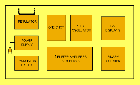
The Logic Designer Block diagram.
The blocks are shown separate, with no inter-connecting lines. This is because each block is independent. They are connected with jumper leads during experiments.
Notice the position of the blocks correspond almost exactly with the blocks on the printed circuit board. Also, if you look at the circuit diagram, the components are in a very similar position to the PC layout. This makes the circuit easy to understand.

The Logic Designer Kit
LOGIC DESIGNER - PARTS LIST
1 - 150R
2 - 220R
2 - 270R
4 - 330R
7 - 470R
2 - 1k
2 - 3k9
8 - 10k
1 - 22k
2 - 47k
4 - 100k
1 - 100n 100v greencap
2 - 1u 16v electrolytic
1 - 1000u 16v to 25v electrolytic
12 - 1N 4148 diodes
4 - 1N 4002 power diodes
1 - FND 500 display
12 - 3mm red LEDs
1 - 3mm green LED
2 - 555 timer IC’s
1 - CD 4024 binary counter IC
1 - CD 4026 decade divider & Driver
4 - BC 547 transistors
1 - 7805 regulator
2 - 8 pin IC socket
1 - 14 pin IC socket
1 - 16 pin IC socket
1 - push button
1 - Heat-fin for 7805
40 - Hollow Machine Pins
1 - nut and bolt for heat-sink
10cm - tinned copper wire
1m - fine solder
20 - 15cm lengths of solid-core hook-up wire
1 - LOGIC DESIGNER PC Board
Note:
- LED - Light Emitting Diode
- FND - Fairchild Numeric Display
Extras:
Jiffy or Zippy box type UB3
ADDITIONAL PARTS
These parts must be bought from you local electronics supplier.
Read through this project completely before ordering any of these parts.
POWER TRANSFORMER
To make a 150mA power supply you will need a transformer type 2851.
This is 240v to 12.6v CT @ 150mA.
If you want 5v or 9v but not 12v out of the power supply, you can get type 2840.
This is 240v to 9v CT @ 150mA.
For a 1 amp power supply, use a transformer type 2155.
This has tapings up to 15v @ 1 amp.
You will also need a power cord and 3 pin plug.

The Logic Designer Printed Circuit Board
CONSTRUCTION
There are two ways of getting the parts required for a project such as this. One way is to search through your parts box for all the resistors and capacitors LEDs and diodes and then go out and buy the missing components. This is both uneconomical and unwise. Most often you don’t have the correct value component and try to make do with the nearest value. Additionally the components are not the same size and the project finishes up looking like a pile of junk. We have seen it so many times with the units sent in for repair.
The most economical and smartest thing to do is buy a kit of components. At least all the parts will co-ordinate and are designed to fit into the spaces on the board. And with all new components the project is sure to work.
Most of the large electronic suppliers will stock the individual components for this project as all the items are standard values and should be readily available.
When you have collected all the components, lay them out on the bench and make sure you can identify each of the values. Start at the left hand side of the board and insert the four diodes. Progress across the board inserting each component as you come to it. The overlay on the board makes it very easy to identify the positioning of the polarized components such as the electrolytics integrated circuits transistors and diodes.
Four jumper links are required near the 7-segment display and these can be made from the ends of resistors.
The overlay on the board should be enough to guide assembly. If you are still unsure, use the overlay of the board. It is most important to correctly position the IC’s and 7-segment display. The notch or dimple on the IC sockets must be positioned so that pin 1 goes down the correct hole.
The FND500 7-segment display has no pin identification and you must rely on looking at the display for the decimal point.
When all the parts have been inserted, go over every component again and confirm that it has been fitted in the correct place and is positioned around the right way. So many times we find transistors and electrolytics incorrectly fitted. It’s always the simplest thing that lets you down.
All that is required now is to fit a power transformer. You should already know the current rating of the transformer you are using and if it has a centre-tapped secondary or a single winding. To power this project and any other circuit you are designing (containing up to 4 or 5 IC’s) I would suggest 150mA to 300mA secondary would be sufficient. This type of transformer can be mounted inside a Jiffy box and the board fitted on top (in place of the lid). This will hide the dangerous 240v leads and give you plenty of mounting room for the transformer.
If you are not 100% certain about wiring up the mains side of the project, I suggest you approach a qualified person to at least inspect what you have done.
This may be your electronics teacher, a friend with electrical know-how or your local electrical shop. Don’t take any risks. Especially with the 3-pin plug and terminal block.
Three-core leads are now required to conform to the new colour coding .This has been mainly designed for colour-blind people as it does not follow any electronic logic. The brown wire is taken to the active pin.
This pin is sometimes identified on the plug so look for it. If you are not sure, the active pin is the left-hand hole of the wall-socket. The blue lead goes to the neutral pin - previously the black lead and finally the green lead with the yellow stripe goes to the earth pin.
This lead should be a little longer than the other two so that no strain is placed on it. This means it will be the last lead to fracture if the cord is tugged.
After checking all the AC side of the transformer wiring and looking over the circuit board for any solder shorts, the power is applied. All the circuits in the LOGIC DESIGNER have been designed for 5v operation. This will enable you to experiment and build up circuits with either CMOS or TTL chips.
All the IC’s in the LOGIC DESIGNER will operate in the range 5v to 12v so we have chosen 5v as being common to both chips.
When the power is applied, the 7-segment display will light up along with the LEDs in the transistor tester. These act as power-on indicators. By their intensity you will know the supply is delivering 5v.
If the LEDs do not light up, check the regulator for temperature rise. If it is getting very hot, you may have a short in the output. For best operation, the power transformer should be rated a 9v. This gives the minimum input-output voltage on the regulator and will create the least amount of heat from the regulator.
If the regulator is still cold, feel the power transformer for overheating. A temperature rise here will indicate a short in the diode bridge or an incorrectly inserted diode.
Don’t forget the possibility of solder bridging two tracks and causing a short circuit. If the LEDs light up you can assume the power supply section is working.
The 555 (nearest the power supply) is connected as a “one-shot”. This means it will produce an output of one pulse every time the push button is pressed. We have already explained on numerous occasions that a push button has contact bounce and no matter how well the push button is constructed, it will send more than one pulse to a digital circuit if it is used by itself. It is absolutely essential that all push buttons are de-bounced.
This entails some sort of delaying circuit so that the closing of the contacts are all grouped together to register as a count of one. The other necessary part of a “one-shot” is the speed with which the circuit changes from a LOW to a HIGH. If the rise time is slow, the digital circuit accepting the pulse will count up to 10 or 100 counts since there is an interval between the LOW and HIGH called the indeterminate zone. If you sit in this area with a voltage of about ½ Vdd the IC will tick over rapidly.
Our ‘one-shot” circuit avoids any of these troubles. It provides a clean pulse with a very high slew rate. All CMOS circuits will see this as one single pulse. To make the de-bouncing even more effective, we have introduced a long delay-time so that you cannot produce any more than about 10 pulses per second.
The secret to making a 555 into a “one-shot” lies in pin 2. By keeping it tied high via a resistor the 555 will be turned off. To turn the 555 on, pin 2 must be brought down to 1/3 of the supply voltage - or less.
When the 555 is sitting ready to give its pulse, pin 7 is effectively connected to ground via the circuit inside the IC. This means the electrolytic will be sitting in an uncharged condition - because pin 6 does not provide any power out of the IC. It only detects the voltage on the electrolytic. When the voltage on pin 2 comes down to ½ of the rail voltage, the IC turns on. The short on pin 7 is removed and the electrolytic begins to charge up via the two resistors.
When the voltage rises to 2/3 of the supply voltage, pin 6 turns the IC off. We are assuming pin 2 has been taken HIGH before the electrolytic has triggered pin 6. If pin 2 is still LOW, the IC will remain turned on and will turn off as soon as the push button is released.
To see the one-shot in action, connect the output of the 555 to one of the inputs of the buffers. Touch the pulse button very quickly. The LED will turn on and remain on for a short time, and then go out. If you keep your finger on the button for a long time you will not see the action of the one-shot. If the LED stays on in this manner, you can be sure the one-shot is operating. Test the other three buffer transistors for similar operation.
If the circuit does not show any delaying action on any of the LEDs, you should try the electrolytic for correct insertion. Also check the value of the timing resistor. By placing a multimeter on pin 6 you will be able to detect the increasing voltage as the electrolytic charges. The output pin 3 goes HIGH when the IC is turned on. It is normally sitting in a LOW condition.
The second 555 is connected in an astable or free-running mode and will produce 10 pulses per second from the output pin 3.
You have three ways of testing this circuit. It can be connected to any of the buffer transistors or the 7-segment readout via the CD 4026 or it can be used to pulse the binary counter IC (CD 4024). If you try all the three methods you will become acquainted with the ways of detecting an output. This just about covers the LOGIC DESIGNER. The only section left is the TRANSISTOR TESTER.
THE TRANSISTOR TESTER
The transistor tester is extremely handy. How many times have you required a lead-out for a particular transistor only to find it unlisted, even in a book of 30,000 types. It always happens. The very transistor you require for a cross-reference is missing from the list. With this very simple device you can test almost any type of transistor and identify its important static characteristics. By this I mean you will be able to determine if it is a PNP or NPN transistor and identify the COLLECTOR, BASE and EMITTER leads. It will also show if the transistor has a short in either junction. The characteristics it will not reveal are its current handling capability, maximum frequency of operation, leakage or gain. These you have to get from data sheets. To operate the transistor tester it is necessary to power the LOGIC DESIGNER from the mains. The 50Hz AC is rectified by the transistor under test to light one of two LEDs. Battery operation would not give this AC input and unfortunately the transistor tester is in-operative with battery power or even when using a battery eliminator such as a plug pack. There is one plug-pack however which has an AC output and this can be used.
The testing of the DESIGNER has now been covered. Make sure it woks properly before using it as a test rig.
VOLTAGE REGULATOR
We have chosen a 7805 voltage regulator to supply this project. It is the cheapest and easiest to fit on the board. If you intend to power other projects from this supply it will be necessary to remotely mount the regulator on a large heat-sink. Under these conditions it would be possible to use the LM 317k 3-terminal adjustable regulator. Since it is in a TO-3 package, it will require 2 screws for mounting and thermal compound for adequate heat conduction. If possible try to avoid a mica insulating washer. This will reduce the efficiency slightly. Keep the heat fin away from any earthing points to preventing it shorting out.
HEAT-SINKING
The heat-sink shown in all the photos is only suitable for dissipating the power requirements of the LOGIC DESIGNER itself. The heat fin will only dissipate about 1 watt.
If you take the case of 12v being supplied to the input terminal of the regulator and 5v emerging from the output, the wattage being lost in the regulator will be very close to 1 watt when 150mA is flowing. Any higher current requirements will overheat the regulator and it may be damaged. I have not had very much success with the current limiting ability of the 7805 in a shorted output mode - it just gets fiercely hot and fails to regulate. Nor does it like to supply any more than a few hundred milliamps into a free-standing heat fin. If you will be requiring more than 500mA for long periods of time you will need to remove the regulator from the board and mount it on a solid piece of aluminium capable of dissipating the excessive heat. When clamping the regulator, use some form of thermal compound and connect fine flex to the three leads to prevent them from fracturing and breaking.
MACHINE PINS
To keep this project inexpensive, we have chosen machine pins for the input and output terminals. These aren’t the best choice in the world as they fracture easily and break off. But if used carefully, they will last quite a long time.
INSERTING THE MACHINE PINS
If you find it difficult holding the Machine pins while soldering, you can make up an inserting tool by soldering a machine pin onto a piece of copper wire which is about 8cm long. This will save burning your fingers.
TESTING THE LEDs
The 13 Light Emitting Diodes are opaque and you can see inside them. The cathode lead is shorter than the anode when you buy the LEDs but how do you tell which is the cathode lead after you have snipped them both to the same length? Since you can see inside the body of the LED, you will find that the cathode lead ‘dog-legs’ over towards the other lead or it is the larger of the two.
On the PC overlay, the symbol for a LED is the same as for a diode. Don’t get mixed up. See the photo and layout diagram before fitting any parts.
After soldering the LEDs into circuit, they should be tested as they can be easily damaged by heat. Use a 6v lantern battery fitted with a 220R dropping resistor to check each LED individually.
IDENTIFYING THE FND500
To identify the decimal point on the display, use a battery and 330R resistor.
If you solder the FND500 into the project around the wrong way by mistake, it will not be damaged. All that will happen is the outer segments will light up in an odd pattern and the decimal point will light in place of the central segment. You will not get any recognizable numbers. So, to avoid having to de-solder the display, check first.
THE PUSH BUTTON
The Printed Circuit Board will accept either a square push button or a new-style push-button. These new buttons look very professional.
They can be soldered either way around as we are using only the diagonally opposite corners for switching.
MEASURING THRESHOLD VOLTAGES
Digital IC’s must have at least ½Vdd (rail voltage) to enable them to clock.
This situation becomes critical when an output is trying to drive a LED and also clock another IC. Normally you would provide a buffer to supply the LED with full illumination, but in our simple project we omitted this luxury. The LED and dropper resistor shown in the diagram will reduce the output voltage of the 4024 to very near ½Vdd and it may be difficult to produce enough swing to drive the 4026. If you find the 4026 does not clock, the 470R resistor can be increased to 560R. This will allow the voltage to rise by about 1v and clock the chip.
DIODES
For this project, almost any 1 amp diode will be suitable. 1N4001 are 50v diodes, 1N4002 are 100v diodes, 1N4004 are 400v diodes and 1N4007 are 1000v diodes.
Since the power supply is only producing 12 to 20v, we can use any PIV rated diode and still have ample to spare.
USING SOCKETS
IC sockets should be used for this project. This will give you the added advantage of being able to test the 555 IC’s, 4024 IC’s and 4026 IC’s. This will also prevent the possibility of damaging the IC’s when they are soldered into the project. lf you mount the FND500 on Machine pins, you will be able to test other FND500 displays for segment luminance. This is very handy when you buy a bag of mixed displays and wish to test them for output before soldering them into a circuit.
LAST MINUTE THOUGHTS
Hopefully, these notes will cover all your questions and problems with building this project. As such, we are not offering a repair service on this board as we think it is not necessary. If you do have any problems with the construction, email the author for assistance. Many people are taking advantage of this service to get them out of a problem.
Take it from me, the board is so simple that the project is guaranteed to work. If you have any trouble with one of the sections, get someone else to follow through your construction - because you will be oblivious to the mistake. This usually comes from incorrectly inserted parts, poor soldering or cooking a component. A good soldering iron is essential. Use a low-wattage type and don’t think of using an instant-heat type.
We built-up a number of these units and they all worked very well. After a little experimenting, one of the staff found a couple of additional uses which I hadn’t thought of. These have been presented in the following section 13 EXPERIMENTS WITH THE LOGIC DESIGNER.
USING THE 240v
Many schools do not permit the construction of mains operated projects when live wiring is required in its construction. That’s where you’ll find the AC Plug-Pack saves the day. At a pinch, some of the other plug-packs can be taken apart and the diodes removed along with the smoothing electrolytic. So you have a number of alternatives to having to wire up a power transformer.
As with some of our past projects, this board is modular. It fits neatly onto a Jiffy box and the transformer can be fitted inside. Don’t forget to add a few ventilation holes to allow the heat to escape and use a cable clamp to keep the power cord from pulling on the wiring.
If you haven’t already realized, this LOGIC DESIGNER is intended to be used with breadboard. These bread-boarding systems have proven immensely popular. The best layout is to stick the bread-board onto the work-bench with a piece of double-sided sticky-tape and place the LOGIC DESIGNER on the far side. This will allow you full access to the bread-board and yet keep close proximity to the LOGIC DESIGNER so that the jumper leads can be kept short.
Included in the kit is a bunch of hook-up wires similar to telephone wire.
Don’t use ordinary hook-up wire as it spreads the contacts in the bread-board and damages the Machine pins in our project.
This just about completes the project. I hope you have as much enjoyment in construction this design-aid as we had in preparing it.
to: Page 1
to: 13 Experiments

Quick Links
Legal Stuff
Social Media