

Table Of Contents

**This is a very large article on 27MHz transmitters and receivers.
3 kits are available:
- 27MHz Field Strength Meter - to test your 27MHz transmitter
- 27MHz Transmitter - 2 Channel - transmits two different tones on a 27MHz carrier
- 27MHz Receiver - 2 Channel - receives and decodes 2 different tones and we have 303MHz and 315MHz links. email Colin Mitchell for details.
Where do you start?
Read all this this article then build the 27MHz Field Strength Meter kit: $6.50 plus $4.00 post
and 27MHz Transmitter - 2 Channel. kit: $6.50 plus $4.00 post
then 27MHz Receiver - 2 Channel. kit $10.50 plus $4.00 post
27MHz Field Strength Meter
Tests 27MHz transmitters
$6.50 plus $4.00 post
Buy: [27MHz FSM kit](mailto:colin@elechelp.com?Subject=Buying 27MHz FSM kit&Body=Please e-mail the cost of sending 27MHz FSM Kit by air mail to my country:**___**** and send details of how I can pay for it. My name is:____)**
27MHz Transmitter - 2Ch
$6.50 plus $4.00 post
Learn about making a 27MHz transmitter and create a 2-Channel link to turn on motors and globes etc.
Buy: [27MHz Transmitter](mailto:colin@elechelp.com?Subject=Buying 27MHz transmitter 2Channel kit&Body=Please e-mail the cost of sending 27MHz Transmitter Kit by air mail to my country:**___**** and send details of how I can pay for it. My name is:____)**
27MHz Receiver - 2Ch
$10.50 plus $4.00 post
This receiver is used with the 2-Channel transmitter above to produce a link to turn on globes and motors.
Buy: [27MHz Receiver](mailto:colin@elechelp.com?Subject=Buying 27MHz Receiver 2Channel kit&Body=Please e-mail the cost of sending 27MHz Receiver Kit by air mail to my country:**___**** and send details of how I can pay for it. My name is:____)**
What will I learn?
You will learn about designing 27MHz stages - transmitters and receivers
You will learn about OSCILLATORS - low frequency and 27MHz
You will learn about TUNED CIRCUITS - how they produce an enormous waveform when operating at a special frequency.
CONTENTS
- [27MHz transmitter with crystal](#THE 27MHz TRANSMITTER) - 1-transistor with crystal
- [Receiver for transmitter](#Receiver for Tx_A)
- [27 MHz transmitter without Xtal](/articles/27mhz-transmitters/page-2#CIRCUIT A) - Very simple 2-transistor circuit - produces tone.
- [Receiver for Transmitter](/articles/27mhz-transmitters/page-2#GS REMOTE CONTROL RECEIVER)
- [27 MHz transmitter without Xtal](/articles/27mhz-transmitters/page-2#CIRCUIT B) - with multivibrator to produce tone.
- [27 MHz transmitter without Xtal](/articles/27mhz-transmitters/page-2#Improved Circuit) - with multivibrator to produce tone - improved circuit
- Receiver for transmitter
- [2 Channel 27MHz transmitter without Xtal](/articles/27mhz-transmitters/page-2#2 CHANNEL TRANSMITTER)
- [Receiver for 2 Channel transmitter](/articles/27mhz-transmitters/page-2#2 CHANNEL RECEIVER)
- [4 Channel 27MHz transmitter](#A MULTI-CHANNEL LINK) with crystal
- [4 Channel 29MHz Transmitter](/articles/27mhz-transmitters/page-2#4 CHANNEL TRANSMITTER) with Xtal
- [4 Channel Receiver](/articles/27mhz-transmitters/page-2#4 CHANNEL RECEIVER)
- [Field Strength Meters](/articles/27mhz-transmitters/page-2#FIELD STRENGTH METERS)
In this discussion we cover 27MHz transmitters and receivers as found in remote control cars, aeroplanes, walkie talkies and some of the older-style garage door openers.
We have provided a number of circuits so you can work out the best type for your application and these circuits will also help you understand which components are critical and which components can be changed.
It’s a matter of looking at each circuit and seeing the general layout, and comparing it to the other circuits. In this way you are building up a concept of “building blocks” and this is the basis to learning electronics.
Talking Electronics does not provide any kits for these circuits as the products (toy cars, wireless doorbells etc) are readily available in toy shops, hobby shops and many of the $2.00 “junk Shops.” You cannot buy many of the special components and the cost of the completed item is less than buying the components!
WHERE DO YOU START?
Surprisingly, the place to start is to build a piece of test equipment called a Field Strength Meter. We will describe 3 different Field Strength Meter circuits. The simplest circuit detects RF from the antenna of a transmitter and provides a reading on a multimeter.
The other two circuits have a tuned front end and as the capacitor is adjusted, the meter increases to a peak then drops as the frequency is passed.
For experimental purposes, it is not necessary to be on the 27MHz band, but it is handy to know if your transmitter is producing an output.
You need a starting point and you either need a Field Strength Meter or Radio Controller car or Walkie Talkie.
You need something to make sure your transmitter is transmitting. It’s a [Field Strength Meter](/articles/27mhz-transmitters/page-2#FIELD STRENGTH METERS).
MAKING A TRANSMITTER
This discussion covers a number of transmitters and receivers. The different circuits show you what is absolutely needed and how different engineers think. Some circuits will work better than others and some have unnecessary components.
Then you will need a receiver.
Some circuits are 1-channel, some are 2-channel and some are 4-channel. Choose the tone that suits your requirement.
First we will go over some background.
Let’s start:
6 bands (or frequencies) were allocated for the 27MHz band,
| Channel | Frequency |
|---|---|
| 1 | 26.995 |
| 2 | 27.045 |
| 3 | 27.095 |
| 4 | 27.145 |
| 5 | 27.195 |
| 6 | 27.255 |
and these were very popular for transmission - especially in countries where transmitting was strictly controlled.
Both 27MHz and 49MHz circuitry produced very low cost devices and they are still available. But you must be careful as some of the latest types are much more sophisticated (and sometimes cost less than the older types).
We will investigate how they work and how they can be modified.
Very little is available on how these circuits work and this article will cover the “building blocks.”
When we use the term “building block” we mean a group of components making up a circuit that carries out a particular function and can be connected to another circuit to achieve a final result. In this way you can create your own project without having to design each of the sections. A typical example is the 5-channel remote control circuit we have modified to produce an on-off action from two of the outputs. You can build these circuits from scratch, but why re-invent the wheel? If you want a 27MHz or 49MHzlink, the best idea is to buy a toy and modify it.
If you want voice communication, get a walkie talkie. If you want a single on-off operation, get a remote control car.
Some remote control cars have up to 5 channels and sell for less than $20.00. You can get everything you need on 2 printed circuit boards, ready for modification, without having to source the components.
Look for 4 function models that require 3v operation for both remote and receiver. The fifth function is “turbo” and is not used in some of the designs. The photo below is the 4(5) function 27MHz remote control car we discussed above:

5 channel remote control car as discussed in the text. It uses only 4 of the 5 channels.
The first two circuits (figs 1& 2) form a single-channel transmitter-receiver link. The second receiver (fig 7) uses a split supply to power a motor in the forward and reverse direction (it uses the same transmitter as shown in fig 1). The third transmitter & receiver, (figs 12 & 22) is a multi-channel design, with a chip in the receiver. Then we cover a 27MHz walkie talkie. This is a 4 transistor model. It uses the same type of super-regenerative front-end as our receiver circuits and injects Amplitude Modulated (AM) audio onto the signal. The result is a very noisy transmission but a very effective way to achieve both transmission and reception with the minimum of components. Most of the parts have a dual function, operating in both transmit and receive mode. This makes the circuit very efficient, component-wise.
Before we start, some of the Japanese transistors have either a very high frequency capability or a very high collector current. These transistors need to have an equivalent for the circuit to work successfully. Here is a list of some of the type you will come across and some equivalents:
| Type: | Gain: | Vbe | Vce | Current | Case | |
|---|---|---|---|---|---|---|
| 2SC3279 | NPN | 140 to 600 @0.5A | 0.75v | 10v | 2amp |  |
| BC327 BC328 | PNP | 60 @300mA | 0.7v | 45v 25v | 800mA |  |
| BC337 BC338 | NPN | 60 @300mA | 0.7v | 45v 25v | 800mA | |
| BC547 BC548 BC549 | NPN | 70 @100mA | 0.7v | 45v 30v 30v | 100mA | |
| BC557 | PNP | 100mA | ||||
| C945 | NPN | 50v | 150mA | | ||
| 1815 | NPN | 50v | 150mA | |||
 | ||||||
| 8050 | NPN | 10v | 1.5A | |||
| 8550 | PNP | 10v | 1.5A | |||
| 9012 | PNP | 500mA | ||||
| 9013 | NPN | 500mA | ||||
| 9014 | NPN | 100mA | ||||
| 9015 | PNP | 100mA | ||||
| 9018 | NPN | 700MHz | 100mA |
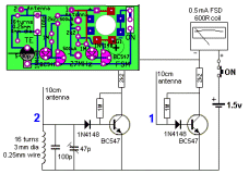
27MHz TRANSMITTER with Crystal
Fig 1 shows a simple 27MHz transmitter producing a carrier.
(receiver for this circuit [HERE](#Receiver for Tx_A))

The 27MHz transmitter PC board

Here is the circuit made by Lucian Papadopol iz6nnh@gmail.com
He has created capacitor values by paralleling two values.
This means it produces an unmodulated 27MHz signal and when picked up by a receiver, such as shown in fig 2, the result is a clean, noise-free reception. To increase the output of the transmitter, the 390R resistor is replaced by a 220R. This increases the current from 7mA to 12mA. The resistor could be decreased to 150R for more output. Page 2 of this article covers test equipment that can be used to detect the output and the frequency of transmission.
MAKING A 5-CHANNEL TRANSMITTER/RECEIVER
This 5-Channel 27MHz link has 5 outputs. The output goes HIGH when the corresponding button on the transmitter is pressed. You can use 2,3 4 or 5 of the channels. We chose 5-Channels as it uses the same number of components as a 2, 3 or 4 channel design.
We will cover the design in detail:
1. The Transmitter 2-transistor, 5-tone (200Hz / 1kHz) transmitter
2. The Receiver “front-end”
3. The receiver
But first:
THE FIELD STRENGTH METER
Before building the Transmitter/Receiver you need to build a Field Strength Meter so you can test the transmitter.
Here is the circuit for Field Strength Meter MkV. It can be constructed on a small piece of matrix board or simply soldered together and connected to a 0-500uA movement. A “Movement” is similar to a “Panel Meter.” You can use 0-1mA movement or the 0.5mA current-range on an analogue multimeter.
This is simply an “untuned” RF detector to prove the transmitter is producing a signal.
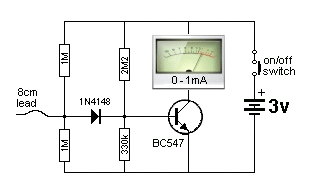
Field Strength Meter MkV
The Field Strength Meter circuit is simple but it is designed to detect the 27MHz transmitter in this project. The “lead” is flex or enamelled wire 10cm long and wrapped around the antenna of the transmitter for 2cm to get RFenergy-transfer. Our prototype transmitter produced about 25% scale deflection.
1. THE TRANSMITTER
The transmitter consists of two transistors. The first transistor produces the tone in conjunction with the second transistor and the second transistor produces the 27MHz signal. Button “A” produces a 200Hz tone button “B” produces 1kHz tone, button “C” produces 1kHz tone button “d” produces 1kHz tone button “E” produces 1kHz tone
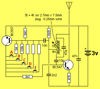
5-tone 200Hz to 3kHz transmitter
The second transistor is a self-contained oscillator and it gets its feedback (to oscillate at 27MHz) from the transformer. The main coil is the 9t section and the feedback to the base is 4 turns.
Nothing happens until one of the buttons is pressed as the first transistor is held in a “turned-off” state by the 3M3 and the second transistor is not turned on as the base and 2k2 are not connected to anything.
When a button is pressed, the 4n7 starts to charge via the resistor connected to the button and the first transistor starts to turn on.
The 4n7 gets charged to a voltage that allow the first transistor to turn on slightly. This allows current and voltage to flow through the 2k2 to turn on the second transistor and produce 27MHz. A voltage-drop is produced across the 100R load resistor and this pushes the left-side of the 4n7 DOWN. The right side moves down and it feeds some of its energy into the base of the first transistor to turn it on MORE.
This causes the second transistor to turn on more and create a higher amplitude. After a very short period of time the energy from the 4n7 (only a small amount of energy is delivered and the amount can be worked out by knowing how many millivolts gets generated across the 100R between normal operation of the second transistor and its higher turned-on state) has been fully delivered and and the first transistor starts to turn off. This causes the second transistor to turn off slightly and the 4n7 “rises in the circuit.” At the same time it gets charged again by the resistor connected to the switch and the cycle repeats.
The end result is a fairly brief pulse that causes the second transistor to create a larger amplitude. This is detected by a receiving circuit as a higher amplitude 27MHz signal produced 200 times or 1,000 times per second. This is called an AMPLITUDE MODULATED SIGNAL and in this case it shown on a CRO as peaks or spikes and in a speaker as a buzz or tone.
The frequency of the tone is determined by the value of the 4n7 and the resistor that charges it.
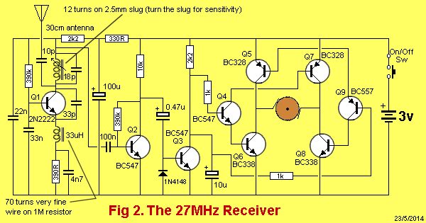
2. THE RECEIVER FRONT END
The front end of a 27MHz receiver is slightly different to the front end of a 27MHz Walkie Talkie. The circuit is very lightly loaded so that it will detect the slightest signal and this makes it very sensitive.
The component that does this is the 3k9 in the power rail.
The transistor has only about 2v across it and takes less than 1mA.
The circuit is a common-base amplifier and under certain circumstances, a single transistor in this configuration will oscillate.
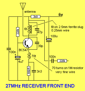

The receiver “front-end” put together for experimenting
First, let’s describe how a common-base stage works.
The 220k base-bias resistor turns the stage on. The coil in the collector is the load but since it is such a low resistance, a voltage-dropping resistor has to be placed in the emitter. This resistor only limits the current through the circuit.
It is by-passed with a 3n3 capacitor and does not cone into the operation of the operation of the circuit.
There are two ways to turn on a transistor.
one is to hold the emitter fixed and deliver a voltage and current to the base. The other is to hold the base rigid and reduce the voltage on the emitter.
that is what we have done in this circuit.
The 4u7 electrolytic on the base holds it rigid and the 39p reduces the voltage on the emitter to turn the transistor ON and during the other part of the 27MHz cycle, it increases the voltage on the emitter to turn it OFF.
This concept must be understood before we can advance further.
The circuit starts by receiving a pulse of current through the 6t coil and 47p capacitor, when it is turned on. These two components form a TUNED CIRCUIT and when they receive energy, they produce a sine-wave (sinusoidal) waveform that appears on the lower part of the tank circuit and this is passed to the emitter via the 39p. It’s an amazing fact that two simple components can produce a sinewave that has an amplitude larger than the voltage applied to the pair, but this is what happens and to fully explain it, would require another chapter.
However the end result is the emitter is pushed down to turn the transistor ON more and pulled up to turn it off. The 70t inductor on the emitter simply keeps it away from the 0v rail so that the pulses on the 39p can have an effect on pushing and pulling the emitter.
To explain how the inductor works is very difficult, however it has the effect of allowing the 39p to push the voltage lower on the emitter, than if it were not included. If the inductor is removed, the 39p will have a very hard job to push against the 3n3. But if the 3n3 is removed the 39p will have little difficulty pushing against the effect of the 680R.
However when the inductor is added, the 39p has a much easier job of pushing and pulling the emitter.
Even though this is the front end of a receiver, it is actually oscillating at 27MHz.
The circuit has been built for experiential purposes to make sure the 70t inductor and 6t coil work perfectly to price a sensitive front-end. Never put a circuit on the web without building and testing it with actual components. Simulation programs cannot predict the outcome of hand-made components.
The 70t inductor is about 7uH and is wound on a 1M resistor with very fine wire. The resistor can be any high value and does not play a part in the functioning of the circuit. It is just a convenient core for the winding. The carbon content of the resistor does not have any effect on the inductance.
3. THE RECEIVER
HOW THE RECEIVER WORKS
The receiver is a super-regenerative design and the output is very noisy. However when a signal of the same frequency as the super-regenerative circuit surrounds the antenna, the circuit has difficulty radiating a signal and it takes more current and less current. These variations appear across the 3k9 load resistor as a change in voltage (a waveform) and the signal is picked off via a 100n capacitor and passed to a filter stage that removes most of the background noise and amplifies the signal (tone).
The following diagram shows just some of the stages needed to decode 5 different tones and deliver the signal to 5 separate outputs:
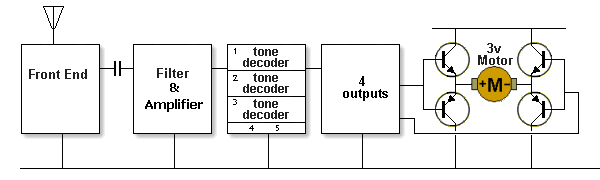
Block diagram of the 5-Channel Receiver
It would require a minimum of 20 transistors to carry out this requirement and all this has been done in a single 8-pin chip by the author, as shown in the following circuit:
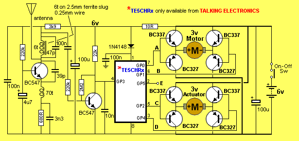
5 CHANNEL RECEIVER using H-bridge transistors
The 5 CHANNEL RECEIVER uses a TE5CHRx chip from Talking Electronics. Click [HERE](mailto:colin@elechelp.com?subject=Buying TE5CHRx IC&Body=Please e-mail the cost of buying TE5CHRx IC by air mail to my country:****___**** and send details of how I can pay for it. My name ) to buy the chip.

Outputs are normally NOT HIGH or LOW but HIGH IMPEDANCE when not activated and this effectively makes them “out of circuit” as far as the other components are concerned.
Outputs A and B produce FORWARD and REVERSE.
When button “A” on the transmitter is pressed, output A goes HIGH and B goes LOW.
When button “B” on the transmitter is pressed, output A goes LOW and B goes HIGH.
Outputs C and D produce LEFT and RIGHT via an actuator (or a motor).
When button “C” on the transmitter is pressed, output C goes HIGH and D goes LOW.
When button “D” on the transmitter is pressed, output C goes LOW and D goes HIGH.
When button “E” on the transmitter is pressed, output E goes HIGH.
The outputs from the chip drive an “H-Bridge” and each transistor is actually an EMITTER-FOLLOWER.
This means the bridge cannot be connected to a supply higher than the driving circuit.
The voltage drops across the driving components is nearly 2v. This means the motor will see a maximum of 4v and that’s why a 3v motor has been suggested.
The chip delivers about 25mA max into the base of each transistor and depending on the gain of the transistor, it will supply about 500mA max.
Output 5 is limited to 25mA.
The H-Bridge section can be designed with an L2930, to take the place of 8 H-bridge driver transistors. The chip has built-in diodes and will deliver up to 600mA per output.
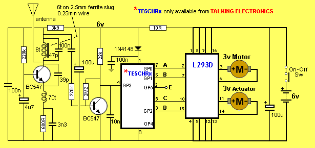
5 CHANNEL RECEIVER using L293D driver IC
(transmitter for this circuit [HERE](#THE 27MHz TRANSMITTER))
In the circuit above, when the transmitter is off, the car moves forward. When the transmitter is on, the car reverses and moves in a circular pattern due to the fact that the front wheels steer straight when the car is moving forward but turn left when the car moves backward. This allows the operator to guide the car around obstacles. It’s a very awkward way to control a car and although it is very simple and clever, it is not really successful in practice. We will not be going into the mechanics of how the car steers, only the fact that the transmitter causes the motor to reverse direction. In place of the motor you could use a relay or two separate motors to carry out a number of functions and we will show how the circuit can be modified to do this.
The receiver works on a “tone,” “no-tone” principle but the transmitter doesn’t actually send a tone as this would require additional circuitry. What happens is the receiver picks up random noise from the airwaves when the transmitter is not operating and this functions as the tone part of the reception. This random noise is amplified by the second transistor and passed to a 0.47u electrolytic that keeps the third transistor in conduction for the majority of the time. The operation of this will be discussed later. The 10u on the output of the third transistor keeps the output low for the short periods when the third transistor is not low. The motor is connected in a bridge formation via four transistors and these change the polarity of the supply to the motor.
When the transmitter is operating, and the receiver is within range, it picks up a 27MHz carrier that over-rides the random noise and produces a CARRIER. This means the second transistor will not see any noise and thus the 0.47u electrolytic will charge and turn off the third transistor. The 10u will charge via the 2k2 and the input to the bridge will change from a LOW to 0 HIGH. This will turn on the opposite half of the bridge to supply current to the motor in the reverse direction.
Now we will cover the circuit in detail.
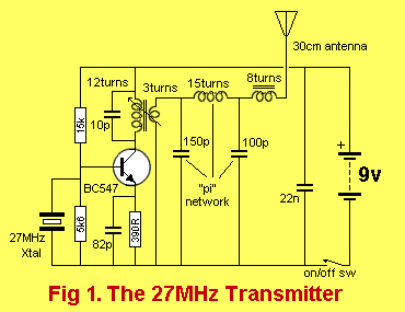
HOW THE TRANSMITTER WORKS
The transmitter is a very simple crystal oscillator. The heart of the circuit is the tuned circuit consisting of the primary of the transformer and a 10p capacitor. These two components oscillate when a voltage is applied to them. The frequency is adjusted by a ferrite slug in the centre of the coil until it is exactly the same as the crystal. The crystal will then maintain the frequency over a wide range of temperature and supply voltage fluctuations. The transistor is configured as a common emitter amplifier. It has a resistor on the emitter for biasing purposes but the 82p across the 390R effectively takes the emitter to the negative rail as far as the signal is concerned. The 390R resistor prevents a high current passing through the transistor as the resistance of the transformer is very low. The tuned circuit operates at exactly the third harmonic (also called the third overtone - an overtone is a multiple of a fundamental frequency) of the crystal so that the crystal will oscillate at its third overtone (27MHz) and in-turn, keep the frequency of the circuit stable. The transformer in the collector of the transistor performs two functions. 1. It matches the impedance of the transistor to the impedance of the antenna, and 2. Creates a resonant circuit at 27MHz to make sure the crystal oscillates at this frequency. You can see the transformer creates a resonant circuit by the fact that it has a capacitor across the primary winding. These two components create a “resonant” or “tuned ” circuit and this is where the circuit “gets its frequency.”
The crystal has a fundamental of about 9MHz and it will oscillate at this frequency unless assisted to oscillate at a higher frequency. This is done by the tuned circuit oscillating at 27MHz.
Now we will look at the impedance-matching feature of the transformer.
The impedance of the output of the transistor is about 1k to 5k and this means it is the impedance (resistance) “it works at.” In other words, it is the characteristic impedance of the transistor in this type of stage. The impedance of a whip antenna is about 50 ohms and the transformer matches these two by having a TURNS RATIO.
The primary has about 12 turns and the secondary about 3 turns. This provides part of the matching requirement. The `pi’ network, made up of the 150p, 15 turn air-cored coil and 100p capacitor assists further in matching the output of the transformer to the antenna. When the power is applied, the transistor turns on fairly hard due to the 82p in the emitter being uncharged.
This puts a pulse of energy through the 10p and as the transistor turns off slightly due to the 82p charging, the energy in the 10p capacitor is passed to the primary of the transformer to start the 27MHz cycle. The action of the emitter rising and falling during start-up, allows the base to rise and fall and this puts a pulse on the crystal to start it oscillating.
The frequency of oscillation OF THE CIRCUIT is generated by the tuned circuit in the primary of the transformer and the crystal merely keeps the circuit operating at exactly 27.145MHz (or 27.240MHz, depending on the frequency of the crystal). The turns ratio of the transformer converts a high voltage waveform (that has little current) from the transistor, into a low voltage waveform with a higher current.
This is exactly what the antenna requires. But before the signal passes into the antenna it goes through the pi network, then an 8 turn Radio Frequency Choke. This is 8 turns of enamelled wire wound on a ferrite core and is called a base-load for the antenna.
The result is a 27MHz frequency called a CARRIER. The carrier produces a clean spot on the band that is free from background noise.
The 22n across the first stage is designed to remove the high-frequency component from the waveform. If this were not present, the circuit would never change state. The receiver is tuned to the frequency of the crystal in the transmitter via a slug-tuned coil in the collector.
When the transmitter is off, the receiver picks up background noise and amplifies it to produce random-noise. This is amplified by the second transistor and passed to the third via a 0.47u electrolytic. This electrolytic is designed to keep the third transistor ON for the major part of the time and it does this in a very clever way. We will assume the supply has just been turned on and the second transistor is not receiving a signal. The 0.47u will be uncharged and it will charge via the 10k collector resistor and the base-emitter junction of the third transistor.
The action of the current flowing through the base of the third transistor will turn it ON but after a short time the electrolytic will be fully charged and the current will cease and the transistor will turn off. A 10u on the collector of the third transistor will then begin to charge via the 2k2 resistor and after a period of time called the DELAY TIME, the output will be HIGH and change the state of the bridge. But if a signal is present on the collector of the second transistor, (in our case this will be background hash), the voltage on the collector will be rising and falling. When the voltage goes low, it takes the positive end of the 0.47u low and the other end must follow.
The voltage on the negative end will go below the negative rail and at -0.7v it gets clamped by the diode. This means the electrolytic gets discharged very rapidly when the second transistor turns on. The result is the electrolytic takes a long time to charge and a short time to discharge, even when random noise (hash) is being processed.
The action of the 0.47u is amazing and will be explained in more detail in a moment. During the short periods of time when the third transistor is not turned on, the 10u on the collector will take over and hold the signal low. It’s only when a long duration of silence is encountered, that the circuit will change state. This period of silence is when the transmitter turns ON and the time is very short in real terms.
Transistor Q3 is called the switching transistor. It changes between HIGH and LOW to create the forward and reverse direction. The switching transistor feeds two driver transistors, Q4 and Q9. Each of these drives two output transistors. Q4 drives Q6 and Q7. Q9 drives Q5 and Q8.
Follow these transistors on the circuit and you will see how the supply is directed to the motor, firstly in one direction and then the other.
The printed circuit board is quite complex because of the number of driver transistors. But since these cost less than 2 cents when bought in the million, it is not cheaper to use a chip.
HOW THE 0.47u WORKS
The 0.47u electrolytic on the base of the third transistor needs explaining as its operation is very clever.
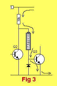
Charging the 0.47u electrolytic is represented as a battery.
The electrolytic is simply a tiny re-chargeable battery and when the circuit first turns on, it is uncharged. The charging current passes through the base-emitter junction of the third transistor and keeps it ON as shown in fig: 3. If the electrolytic is allowed to fully charge, the current will fall to zero and the third transistor will turn off. But the second transistor discharges the electrolytic quickly before it has time to fully charge. It does this by turning ON. How the electrolytic discharges is shown in fig: 4. The only components involved in the discharge are Q2 and the diode. Transistor Q2 is turned on and it will have zero volts (0.3v) on the collector.
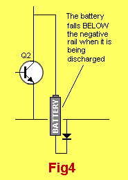
Discharging the 0.47u electrolytic.
This means the positive lead of the electrolytic (equivalent to the positive terminal of the battery) will drop from say nearly 3v, to 0.3v. The negative lead must follow and normally it would be at -2.7v. Yes, the negative lead would have a negative voltage on it relative to the 0v rail, if the diode was not present. BUT the diode on the negative lead gets turned on as soon as the voltage on the negative lead falls to -0.7v and prevents it going below -0.7v. As the positive lead falls, the energy in the electrolytic is quickly discharged through the diode and when the second transistor turns OFF, the electrolytic is ready for charging, through the 10k resistor.
LOW RAIL VOLTAGE
One of the problems of a low rail voltage is the voltage lost across each of the output transistors. Each drops about 0.5v across the collector-emitter junction and this leaves only about 2v for the motor. However the supply voltage must not be increased above 3v as there is a very short period of time when the circuit is changing from LOW to HIGH and both halves of the bridge are ON. This is at the mid-point of the change-over and if you work out the various voltage drops across the base-emitter junctions, it leaves about 0.2v for the two 1k resistors. With a 3v supply, the base current is limited to 0.1mA by the inclusion of the two 1k resistors and 10mA for the collector-emitter current. But if the voltage is increased above 3v, the current will increase dramatically and the transistors will be damaged.
CONNECTING A RELAY
Fig: 5 shows how a relay can be connected to the driver transistor to operate when the transmitter is switched on. The change-over contacts on the relay can be used to power any device when the transmitter is off or when it is on.
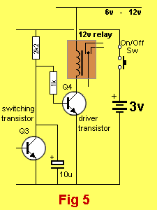
Connecting a relay to the driver transistor. The supply for the relay can be 6v - 12v.
CONNECTING TWO MOTORS
Fig: 6. shows how to connect two separate motors to the circuit. The motors can be connected to any voltage from 3v to 12v and the direction of rotation will depend on which way around they are connected, but transistors Q4and Q7 should be kept at 3v - especially Q9, as it cannot be taken to a voltage higher than 3v, due to the way it is connected in the circuit.
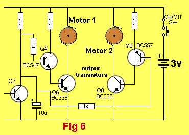
Connecting two motors to the outputs.
A SPLIT-SUPPLY RECEIVER
The second receiver circuit we will study uses more components to do exactly the same job but it may have better sensitivity due to the inclusion of one extra stage of amplification and the use of a higher rail voltage. The higher rail voltage gives some stages a higher gain due to the higher amplitude of the signal. But some of the gain has been lost in the diode pump as this type of pump requires more energy to charge the 10u than a 0.47u. The use of a center-tapped voltage source saves two transistors in the bridge network but necessitates the use of a double-pole switch to disconnect both halves of the supply.
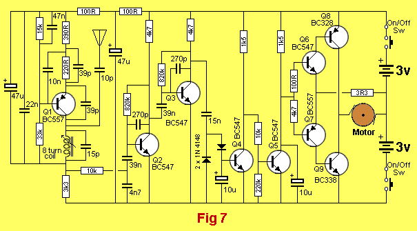
A 27MHz receiver using a split supply

The 27MHz receiver PC board
HOW THE SPLIT-SUPPLY RECEIVER WORKS
The operation of the front end of the split-supply receiver in fig: 7 is identical to the receiver shown in fig: 2. The use of a PNP transistor for Q1has simply turned the circuit up-side-down however the antenna is still connected to the collector and the parallel tuned circuit is also on the collector.
The circuit is turned on by the 33k on the base and the 47n keeps it rigid and turns the stage into a common base configuration. The parallel resonant circuit made up of the 8-turn inductor and 15p, starts the circuit oscillating and the 39p between collector and emitter provides feedback for the transistor to supply pulses of energy to the tuned circuit to keep it oscillating.
The 220R and 39p are the emitter biasing components, as well as the 390R, 10n and 47n. The 100R and 47u are stage-separating components to remove low-frequency noise from the power rails and the 22n across the first stage tightens up the power rails as far as the high frequency is concerned and allows the low-frequency component to appear across the 3k3. The signal across this resistor is picked off via the 10k/39n combination and passed to two stages of amplification.
The 10k and 4n7 form a filter to remove high frequency pulses. A high frequency pulse will try to charge the 4n7 and most of the amplitude of the pulse will be lost (attenuated) in the 10k resistor. Exactly how this works is as follows: The high-frequency pulse will rise and fall before the 4n7 has time to charge. But a low-frequency will charge the 4n7 and enter the 39n for amplification by the rest of the circuit. Going back to the first stage, we have already mentioned that it is oscillating at 27MHz and the MOST ACTIVE lead of the circuit is the collector and this is where the antenna is connected. The waveform produced by the circuit is passed to the antenna and radiated to the surroundings.
Any other signals of the same frequency will interfere with the circuit’s ability to radiate energy and this is reflected down the antenna to the first stage. The result is it takes slightly more and less current according to the intelligence on the signal. The word intelligence means the information that has been added to the carrier.
For a transmitted signal this means voice or music etc. When no transmitted signal is present this is background hash or “noise.” The changes in current will see a waveform develop across the 3k3 feed resistor. The 10k will detect this and pass it to Q2 for amplification. Q2 and Q3 amplify the low frequency (audio) or “hash” component.
Any high frequency signals will be removed by the 270p capacitors. They act as negative feedback devices and operates as follows: A rising signal on the base of the transistor turns it ON and the collector voltage falls. The fall in voltage is passed through the 270p (because it does not have time to charge) to the base where it counteracts the original signal.
The capacitor ONLY has an effect on high frequency signals and the low frequency signals are amplified without attenuation. A low-frequency signal will charge the 270p and get lost in the 270p. After two stages of amplification, the signal appears at a diode pump made up of a 15n capacitor, two diodes and a 10u electrolytic.
The charging of the 10u takes quite a number of cycles as the 15n is like a teaspoon filling a glass with water. When Q3 turns off, the 15n is charged via the 4k7, D2 and the 10u. The 15n doesn’t take very long to charge and the current flowing through it puts a tiny amount of charge into the 10u. Transistor Q3 turns on and discharges the 15n through diode D1 in exactly the same manner as explained previously. When Q3 turns off, the 15n is ready to charge up again. This keeps happening for hundreds of cycles, each time the voltage on the 10u gets slightly higher.
At a voltage of 0.65v, the base of Q4 begins to turn on. Below this value the base does not see anything, and does not have any loading effect on the electrolytic. But at exactly 0.65v a tiny amount of current begins to flow into the transistor to turn it on. The electrolytic keeps charging and as the voltage rises to 0.66v, 0.67v, 0.68v, 0.69v, the transistor turns on more and more. At 0.7v, the transistor is fully turned on and any voltage over this simply spills into the base and is passed to the negative rail via the base-emitter junction. This means the voltage on the 10u does not rise above 0.7v.
To keep the transistor turned on requires a small amount of current into the base and the electrolytic supplies this current. In doing so, the energy in the electrolytic gets used up and the voltage across it reduces.
As the voltage falls, the transistor gets turned off. When the voltage drops below 0.65v, the transistor is fully turned off and does not see any voltage below this. This means the operating voltage for the electrolytic is between 0.7v and 0.65v. Q4 feeds Q5 and when Q4 is turned on, the voltage on the base of Q5 is below 0.65v and it is turned off. The 10u on the collector of Q5 charges via the 1k5 and when it is above 3.7v, driver transistor Q6 turns on and output transistor Q8 operates the motor.
There are two outputs. One drives the motor in the forward direction and the other drives it in reverse.
THE TRANSISTORS IN THE FORWARD DIRECTION
There are two transistors for the motor in the clockwise (forward) direction, as shown in fig: 8.
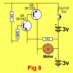
You will notice the turn-on resistor(s) on the base of the driver transistor is lower than for the reverse direction and this will allow a greater current to be delivered to the motor to give it full speed in the forward direction.
THE TRANSISTORS IN THE REVERSE DIRECTION
There are 3 transistors driving the motor in the reverse direction, as shown in fig: 9.
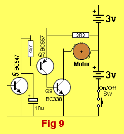
These are the switching transistor Q5, the driver transistor Q7, and the output transistor Q9. The reason why a driver and output transistor are need is to provide a high current for the motor as it needs a high current at start-up or when under load. A motor may take only 50-150mA when not loaded but the current will rise to 300-500mA when loaded. It the motor does not receive this high current, it will appear the car has no power. For the output transistor to deliver this high current, the base must receive a current according to the gain of the transistor.
The gain of a transistor varies enormously, depending on the current flowing through the collector-emitter circuit. The DC gain of a transistor is generally specified as between 100 - 450, but this is under ideal conditions and is determined at a collector current of about 1mA! When the current is increased, the ability of the transistor to amplify decreases. For a small signal transistor, this may decrease to a gain of 75 for 50mA or as low as 10 or 20 for 250 - 500mA.
That’s right, the transistor may only have a gain or 10 or 20 when passing a heavy current. This means the base must receive a current of 25mA to 50mA to make certain the transistor will deliver 500mA. When the transistor turns on fully, the voltage between the collector and emitter is only about 0.2v to 0.5v. If the base is not supplied with sufficient current, the transistor will not turn on fully and the voltage across the collector-emitter leads may be 0.6v or higher.
This is how the transistor limits the current to the device it is powering. For our application we do not want any extra voltage to be lost across the transistor and so it must be fully turned ON. So we want the driver transistor to deliver 50mA. This will be a low-current device and 50mA will be its maximum rating. We can allow a gain of 100 for this device so that it requires a current of 0.5mA into the base to turn it on fully.
The turn-on resistor is the 4k7 and when you take off the voltage drop across the collector-emitter of the switching transistor and the base-emitter junction of the driver transistor you have about 2v remaining from the 3v supply. This gives a base current of 0.4mA.
This is not enough to supply the motor with full current and thus the motor goes slightly slower in the reverse direction.
THE ADVANTAGE OF A SPLIT SUPPLY
With the split-supply design there is no part of the cycle when both outputs are on at the same time. This makes it a much safer design than the receiver in fig: 2. The section of the circuit we are looking at, to see if both outputs are on at the same time, is shown in fig: 10.
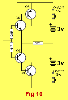
Determining if both outputs are on at the same time.
When the switching transistor (Q5), in fig: 7, is changing from high to low, there is a gap of about 1.2v where both outputs are off. Driver Q6 is tuned on when the input line is above 3.6v, and driver Q7 is turned on when the input line is below 2.4v.
SIMPLIFYING THE SPLIT-SUPPLY CIRCUIT
There are some unnecessary components in the circuit of fig: 7 and by clever re-designing, these can be eliminated. This seems surprising for a mass-produced item but sometimes the designer has not carried out the final step of a design. This is to look at each component and say “Is this part necessary?” If you are not sure, remove it and check the operation of the circuit. If the circuit operates ok, the component may not be necessary. There are 10 components in the circuit of fig: 7 that can be removed and a further 5 can be changed in value when a re-design is carried out. The result is shown in fig: 11.
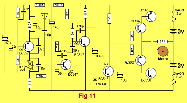
The 27MHz single-channel receiver with the author’s modifications.
The first two components to be removed are the 390R and 10n on the emitter of the first transistor. The 220R is increased to 680R as shown in fig: 11 to produce the same biasing. The reason why the 10n can be removed is because it is effectively across the 390R (via a 47n) so that the join of the 220R and 390R is effectively at rail impedance to high frequencies.
This means the 39p can be connected to the positive rail and the 390R can be incorporated with the 220R. By using 470p as the high frequency filtering component in each of the two audio amplifier stages, the 10k and 4n7 filtering components can be eliminated. It may also be possible to remove one of the audio amplifier stages when the 0.47u electrolytic is used as it is much more effective than the 15n charging the 10u.
The 15n and one of the diodes is not needed when the charging electrolytic is 0.47u. The switching transistor Q5 is not required, however it does invert the signal so that when it is removed, the resistors to each of the driver transistors must be changed so that the output driving the car in the forward direction delivers full power and the reverse output delivers about 80%.
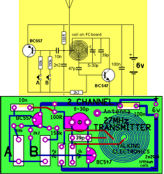
2-CHANNEL LINK $10.00 from Talking Electronics
A number of 2-Channel 27MHz links are available on the web as pre-built modules at very low cost.
They are intended for remote control cars but the trend is now for 4 or 5 channel links, so these are available for $10.00. Email Colin Mitchell to buy a Tx/Rx link And get a 27MHz FSM to test the output for $6.50
You may want to control something at the far-end of a model railway layout and running cables may be practically impossible.
Or you may want to control something that moves around your layout.
This is an ideal way to solve the problem. The range is about 10 metres (tested with 3v on the transmitter).
The modules come with whip antennas - spring-steel wires.


The resistors are different to the markings on the board
The first surface mount transistor is “CR” (2SC945)
The second surface mount is an oscillator chip - not a transistor!!!
This saves about 8 components.
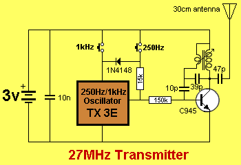
The diode simply prevents the 1kHz switch delivering a voltage to the output of the IC. It does not have any effect on producing the 250Hz signal. It is just a “gating diode.”
The 3-pin chip could be a very small microcontroller that has been programmed to produce 250Hz when it detects a voltage on the output pin. The appearance of the 250Hz indicates the output is generated by a higher frequency and is divided-down.
With 15k, the output has some 1kHz segments in the high part of the waveform when 250Hz is being delivered. With 1k5, the top of the 250Hz waveform is very smooth.
This IC replaces at least 10 components in a two-transistor square-wave arrangement and this saves time, space and money.
The surface-mount transistor produces the 27MHz carrier when the 1kHz from the IC is HIGH. This is because the 1kHz turns the transistor ON during the HIGH periods of the waveform.
The oscillator produces a sinewave and the feedback is the 10p.
The 39p is effectively across both windings and this forms a tuned circuit with a frequency of 27MHz.
A tiny amount of this waveform is picked off by the 10p and passed to the base where the signal delivered to the base turns the transistor ON more and more until it cannot turn on any more. At this point in the wave, the signal via the 10p ceases and the transistor turns off. The collapsing magnetic field delivers its energy to the 39p to charge it and this creates the second half of the waveform. And the signal from the 10p is opposite to previously and it has no effect at all on the transistor. The transistor plays no part in this portion of the wave. Adjusting the ferrite core changes the frequency slightly and this is done when the transmitter is a long way from the receiver so you can detects when the transmitter is operating at exactly the correct frequency. You use the weak reception to make the final adjustment.

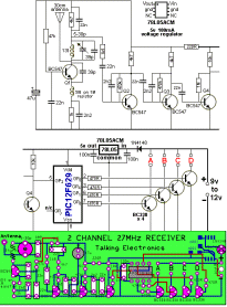
The receiver board

The receiver is just two IC’s and a few surrounding components
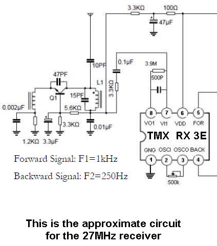
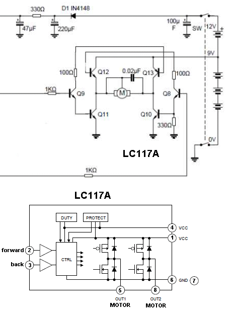

The two outputs can be used to reverse a motor or each output can be used to turn ON a device.
When there is no transmission (reception) both outputs have zero volts.
For Forward, one output goes high and the other goes low.
The voltage lost across the output FETs is only a few millivolts (about 3 to 5mV).
The output FETs can handle about 200mA to 300mA.
Each output can be used to turn ON a separate motor:

You don’t have to buy these modules. You can use the transmitter/receiver from a toy car that no-one wants any-more. (some of them are 4 channel).
You can operate sound modules, lights, gates, points and anything up to 6v and 200mA.
Every module is different with different circuitry and chips. This discussion is just an example of how the link works.
The LC117A chip, TMX RX 3E chip and TX 3E IC are not available.
A MULTI-CHANNEL LINK
A multi-channel link is considerably more complex than a single channel design but it offers the possibility of designing a project that has more features. The multi-channel transmitter shown in fig: 12 has forward, stop, reverse as well as left, centre, right steering.
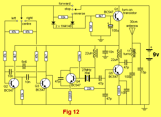
A multi-channel 27MHz transmitter
This represents 6 channels and they are created by changing the mark-space ratio of a square wave oscillator as well as its frequency.
The photo shows the components on the PC board:

The 6 (4) channel transmitter board
When the transmitter is not operating, the receiver picks up hash (background noise) and no outputs are activated. This represents the STOP function. When the forward function is selected on the transmitter, the square-wave oscillator operates at its high frequency setting, with an equal mark-space ratio.
If left-turn is selected at the same time, the mark-space ratio is altered to 1:3 while the frequency remains the same. If right-turn is selected, the mark-space ratio is 3:1, with the same frequency. If the reverse function is selected, the frequency of the oscillator is reduced to half and if the centre steering is selected, the mark space ratio is 1:1. If the left steering is selected, the mark-space ratio is 1:3 and if right steering is selected, the mark-space ratio is 3:1. To understand how the channels are produced, you need to know how a multivibrator works.
HOW A MULTIVIBRATOR WORKS
The multivibrator in the transmitter consists of transistors Q2, Q3 and the surrounding components. This is shown in fig: 20.
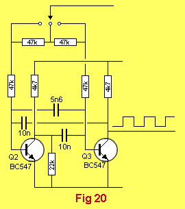
You will notice the symmetry of the circuit and this produces an output waveform that is either HIGH or LOW. The circuit changes from one state to the other very quickly and this produces the fast rise and fall of the waveform and thus its square nature. The HIGH part of the waveform is called the Mark and the LOW is the Space, as shown in fig: 15. A square wave with a 1:1 output has the length of the mark equal to the space.
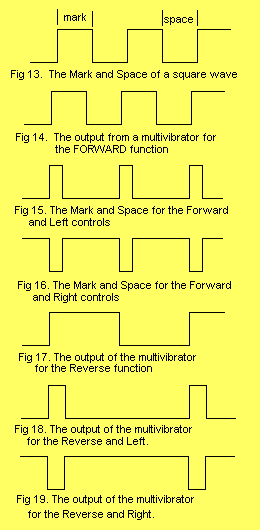
For the transmitter in fig: 12, the output of the multivibrator for the Forward function is shown in fig: 14. We can take this as the reference waveform as all the other waveforms will be a multiple of this. For instance, if the left-turn is selected while in the forward direction, the waveform changes to that shown in fig: 15.
Note the short period of time the waveform is HIGH compared to the LOW time. If this waveform is passed into an integrating network, the percentage of time it is high can be determined and an output activated. This is what the chip does in the receiver.
It determines one of six functions and produces outputs to steer the car in the left or right direction and/or drives the car in forward or reverse. It also detects when the transmitter is not operating and stops the car. If the forward-and-right controls are selected the waveform is shown in fig:16.
When reverse is selected, the multivibrator operates at half the frequency due to the 82k resistor added to the base of the two transistors in the multivibrator. The resulting waveform for reverse is shown in fig: 17. If reverse-and-left is selected, the waveform is shown in fig: 18. If reverse and right is selected, the waveform is shown in fig: 19.
THE TURN-ON CIRCUIT
The transmitter doesn’t have an on-off switch. It is turned on when the forward-reverse control is moved from the stop position. This switches a diode into circuit. The diode charges the 100u via the 4k7 to turn on the emitter-follower transistor Q1. The base rises to just below rail voltage and the emitter is about 0.7v below this. The emitter becomes the power rail for the rest of the circuit and while the controls are in the forward or reverse direction, the circuit is supplied with voltage and current.
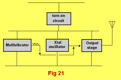
Block diagram of multi-channel transmitter.
The turn-on circuit supplies current to the rest of the circuit when the controls are activated.
When the control is returned to the stop position (via a spring-return), the current required by Q1 to keep it turned on is supplied by the 100u on the base and as the energy is delivered from the electrolytic, the voltage across it reduces. This reduces the voltage across the circuit but since it is not sending out a signal, this does not matter.
After a minute, the voltage drops to almost zero and the electrolytic is finally discharged completely by the 1M (and 4k7 in series with it). The stand-by current drops to less than 1 micro-amp, the leakage through the collector-emitter junction when the transistor is not turned on.
MORE ON HOW THE MULTIVIBRATOR WORKS
Transistors Q2 and Q3 form a multivibrator and the operation of this is fully covered in our books titled Learning Electronics Book 1 and Book 2. The circuit is basically regenerative in which one transistor turns the other off then the second turns the first off. When the circuit is first turned on, both the bases are pulled high via the 10n capacitors but one of the transistors turns on before the other and robs it of turn-on voltage. But the transistor cannot stay turned on forever as the 10n capacitor becomes charged and as it turns off, it sends a pulse to the other transistor.
The second transistor turns on and completely removes the turn-on voltage from the first transistor. Eventually the second transistor cannot remain fully turned on due to the 10n becoming charged, and starts to turn off. This sends a pulse to the first transistor and it starts to turn on. Each transistor has a gain or amplification factor of about 100 and when we say one transistor begins to turn off slightly, this change is passed to the base of the opposite transistor and the result is magnified 100 times on the collector. This is then passed to the base of the first transistor and suddenly a tiny signal gets passed back as a huge signal. That’s why each transistor reacts so quickly and the result is a very fast change from one state to the other. This is shown in the shape of the output waveform.
The rise and fall times are very short and the sides of the square wave are very steep. The frequency of the output is determined by the value of the components on the base. This includes the base resistor and the capacitor connecting to the opposite transistor. In the circuit of fig: 12, the capacitors are fixed at 10n and the resistors are changed.
An increase in resistance causes the capacitor to take longer to charge and decreases the frequency of the circuit. The output of the multivibrator is passed to the base of the RF output transistor where it controls the on/off time for the transmitter. When the transmitter is turned on, a 27MHz frequency is injected into the base of the RF output transistor via a 47p from the crystal oscillator. This crystal oscillator is made up of transistor Q4 and its surrounding components.
The transistor is turned on via the crystal and 22uH inductor. The crystal is equivalent to about 20p and the resistance of the inductor is about 1 ohm. The emitter is held fairly rigid via the 47p and the transistor gets a very short pulse from the crystal. This puts a pulse of current through the coil and the current creates magnetic flux. As soon as the pulse ceases, the magnetic flux collapses and the inductor produces a voltage in the opposite direction and passes the waveform through the 47p to the base of the RF output transistor. It also passes the waveform through the crystal to turn off the oscillator transistor Q4. When the transistor is turned off, it does not put any load on the inductor and the amplitude of the waveform is fairly large. After a short period of time, this waveform ceases and the transistor gets turned on by the 120k base bias resistor.
This injects another pulse of current into the inductor and the cycle repeats. The inductor creates the time delay for the waveform as it takes time for the current to convert to magnetic flux then back into a voltage in the opposite direction. This time-delay approximates to about 27MHz and the crystal locks it on to the frequency of 27.240 by exhibiting a larger capacitive effect at this exact frequency. This is how the circuit is pulled into line and kept at an exact frequency, even though the supply voltage may decrease or the temperature may rise.
The 27.240MHz waveform is passed to the RF output transistor and the transistor is turned on and off at the frequency of the multivibrator. The transistor is in common emitter mode as evidenced by the 10n on the emitter.
The impedance of this capacitor at 27MHz is very small compared to the 100R and the emitter considers it is connected to the negative rail as far as the high frequency is concerned. The 27MHz waveform on the base is amplifier by the transistor and appears on the collector in magnified form.
The 22uH inductor on the collector prevents the signal passing to the power rail. It does this by producing a “back-voltage.” As the transistor turns on, the current through the inductor increases and magnetic flux is produced in the coil that cuts the other turns of the coil and this induces a voltage and current in them that is in opposition to the current being delivered. The result is a reverse voltage is produced that makes it difficult for the forward voltage to enter the coil.
This means the forward voltage gets larger and larger in an attempt to enter the coil and the result is a large voltage appearing on the collector of the transistor. This voltage passes through the 47p to a tuned circuit made up of a 11 turn inductor and 15p capacitor. These are designed to match the high impedance of the output of the transistor to the low impedance of the whip antenna. Matching is required to get the maximum signal to pass into the antenna. This completes the coverage of the sections in the transmitter.
THE MULTI-CHANNEL RECEIVER
The signal from the transmitter is picked up by the receiver as bursts of tone between hash. Viewing the signal on a CRO (Cathode Ray Oscilloscope) will look something like fig: 23.

The signal from the multi-channel transmitter will consist of a regular waveform between background hash.
The receiver is required to pick out the signal from the noise and it does this by a process called integration and differentiation where the signal is detected due to its regular nature and this is used to charge a capacitor.
Another circuit determines the length of time the tone is present and these are combined to determine the nature of the control signal. Most of the circuitry for doing this is locked inside the chip in the receiver and the only components we can see are the external items on pins 10, 1 and 19. These determine the frequency detected by the chip and the length of the “highs,” but all the rest of the signal processing is done inside the chip. The chip detects the waveforms shown in figs 14 - 19 and turns on the appropriate outputs.
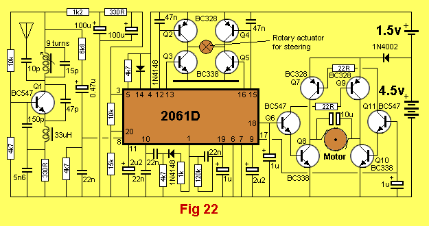
A multi-channel 2MHz receiver

The 27MHz receiver PC board
Two outputs drive the motor in the forward/reverse direction and 4 outputs drive the transistors for the steering motor. The steering motor is simply a rotary actuator. This is similar to the armature of a motor, positioned inside a circular magnet.
The armature does not need brushes as it will only turn about 45° in one direction and 45° in the opposite direction, depending on the direction of the current. The output of the shaft will be connected to a lever to steer the front wheels.
The chip controls the two diagonally opposite transistors for the clockwise and anticlockwise rotation to get left and right steering. All the rest of the circuit has been previously discussed and the only new feature is the tapping at 4.5v for the motor. A diode on the 4.5v rail drops the voltage to 3.8v and the two output transistors drop a further 1v, so that motor receives about 2.8 to 3v.
Here are some remote control items, shown on the web, by a hobbyist who disassembles devices and makes a new project:

Some of these components were used to build a project and present it the web.
A 27MHz WALKIE TALKIE - An Overview
Walkie Talkies are the next logical step in this discussion. They show how a crystal oscillator can be used to transmit voice. Transmitting a voice via a crystal locked oscillator is not easy. This is because the crystal is locking the frequency and it is very difficult to shift it. The only way to do it is to add the audio as an amplitude component so that the amplitude of the oscillator rises and falls with the audio signal but its frequency does not change.
The only problem with this mode of transmission is interference. Electrical noise entering the airwaves is also a varying amplitude waveform and the receiver will pick this up at the same time and produce a very noisy result. This is one of the reasons why walkie talkies are so noisy. However it is a starting point for learning about transmission and the circuit in fig: 24 shows how the audio is added to the carrier.
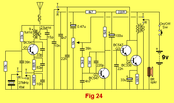
A 4-Transistor Walkie Talkie
Nearly all the components in the 4-transistor circuit are used for both transmitting and receiving. This makes it a very economical design. The frequency-generating stage only needs the crystal to be removed and it becomes a receiver.
The operation of this circuit coincides with our discussion on receiver circuits at the beginning of this article where we said the receiver was oscillating all the time, similar to a weak transmitter. A 390R is added to the emitter of the oscillator stage to reduce the activity and turn it into a receiver. The next section of the circuit is called a building block.
It consists of three transistors directly coupled to produce an audio amplifier with very high gain. The first transistor is a pre-amplifier and the next two are wired as a super-alpha pair, commonly called a Darlington pair to drive the speaker transformer.
The third block is the speaker. This is a separate item because it is used as a speaker in the receive mode and a dynamic microphone in the transmit mode. A speaker can be used in reverse like this and it is called a dynamic microphone because of the coil and magnet arrangement. When you talk into the cone, the movement of the voice coil in the magnetic field produces a few millivolts output. This can be coupled to a high gain amplifier to get quite good results.
When the walkie talkie is in the receive mode, the first transistor is configured as a receiver and the audio is picked off the 4k7 load resistor via a 0.47u electrolytic. It then passes through a volume control and into the three transistor amplifier. The speaker transformer couples the amplifier to the speaker and we hear the result. When the walkie talkie is in the transmit mode, the speaker is placed at the input of the audio amplifier.
The audio is then amplified and the waveform appears as THE SUPPLY VOLTAGE FOR THE TRANSMITTER STAGE. The crystal is connected to the first stage and the gain of the transistor is increased by removing the 330R and only using a 56R for the emitter resistor.
The speaker transformer is not used as a transformer in this mode but as an INDUCTOR to couple the output of the audio amplifier to the power rail and the signal developed across the winding is passed to the transmitter stage as the supply voltage for the transmitter. As the waveform rises and falls, it changes the gain of the first stage and thus the amplitude of the transmitted signal. This is how the signal becomes an Amplitude Modulated (AM) Radio Frequency (RF) signal.
THE WALKIE-TALKIE CIRCUIT IN DETAIL
In the receive mode, the first transistor is configured as a low-level oscillator. The base is tied to earth via a 39n capacitor. This makes it a common-base configuration and the gain of the transistor is high. The input (the collector) is also high, whereas the input (the base) of a common-emitter stage is medium to low.
If this type of stage were used, the antenna would not be as sensitive in detecting up a signal. The feedback for the transistor is provided by the 33p between collector and emitter. The emitter has a 330R and 56R in series to keep the gain low.
The circuit starts up and oscillates due to a tuned circuit on the output of the RF transformer. The transistor detects this oscillation on the primary side of the transformer and passes the signal to the emitter via the 82p, where the gain of the transistor increases the amplitude of the signal to a medium level. If the amplitude is too high, the stage will not be responsive to the surrounding signals.
Any nearby signals of the same frequency will increase and decrease the current taken by this stage and the information on the signal will appear across the 4k7 load resistor as a varying voltage. The 0.47u picks off the voltage and passes it as an audio signal to the volume control and finally the 3-transistor amplifier. The 4n7 between base and ground of the first amplifier transistor is designed to remove any high frequency signals and the output of the transistor goes to a super-alpha pair to drive a speaker transformer.
The speaker transformer matches the output of the transistor to the 8 ohms of the speaker. Matching is done by the transformer having a turns ratio. It has 525 turns for the primary and 75 turns for the secondary. The purpose of the transformer is to convert a high voltage (about 7v), with low current to a low voltage (about 400mV) at high current. This is what the speaker requires. It needs a high current to pull the cone into the magnetic field. The remaining components are biasing components or capacitors to remove the high-frequency signal.
SETTING THE BIAS FOR THE 3-TRANSISTOR AMPLIFIER
The circuit in fig: 25 shows the components that set the bias for the three transistors.
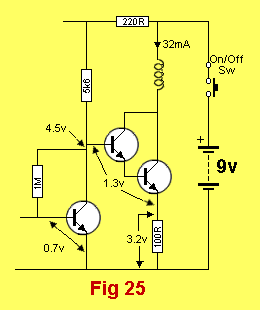
The biasing of the 3-transistor amplifier
All the other components have been left out because they do not determine the DC bias point. The biasing starts at the base of the first transistor. It is turned ON, but not fully, by the 1M resistor until the collector voltage falls to half-rail voltage. The 1M and 5k6 resistors are chosen so that this occurs.
This is the ideal set-point so that the pre-amplifier transistor can amplify both the positive and negative excursions of the signal without distortion. The super-alpha pair (the second and third transistors in the 3-transistor amp) drops a total of 1.3v across the base-emitter junctions, leaving 3.2v across the 100 ohm emitter resistor. By ohms law, this will produce 32mA as the idle current (quiescent current) for the audio stage.
Here is a hand-cranked walkie talkie:

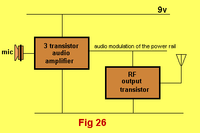
The walkie talkie in transmit mode. The signal passes from the audio amplifier to the RF stage via the power rail
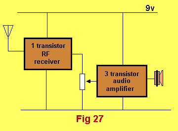
The walkie talkie in receive mode. The circuit is conventional with the first stage feeding the 3-transistor amplifier via a volume control
THE EMITTER BY-PASS CAPACITOR
The 33u electrolytic on the emitter is called the emitter by-pass capacitor. It connects the emitter to the 0v rail when the stage is processing a signal and the signal by-passes the 100 ohm resistor. To see how the electrolytic works we firstly have to remove it and see why the Darlington pair has NO GAIN. Refer to fig: 25. When a signal is fed into the base of the pre-amplifier transistor it will be amplified about 100 times and appear on the collector. Suppose the collector voltage rises 5mV.
This will be passed to the base of the top transistor of the Darlington pair and since it is almost fully turned on, the emitter will rise too. The emitter of this transistor is connected to the base of the lower transistor and the base will pull the emitter up too.
The collector voltage will not change and this means the transistors will produce NO gain because the voltage on the emitter is allowed to rise. It we hold the voltage on the emitter rigid, the pair will give us gain. To do this we connect an electrolytic between 33u and 100u. It has the feature of taking a long time to charge (and discharge) - compared with the rise and fall time of the signal.
When the 5mV waveform appears on the base of the Darlington arrangement, the base tries to rise but it is fixed by the characteristic voltage of 0.7v developed across each of the base-emitter junctions. The result is the base rises 0.1v and both transistors get turned on more. The resistance between the collector and emitter of the output reduces and the transistor allows more current to flow through the primary of the speaker transformer.
THE SPEAKER TRANSFORMER
A lot of discussion could be devoted to the operation of the speaker transformer as the design of a transformer is very complex. There are two ways you can design a transformer. One is to calculate the requirements from scratch and the other is to copy an existing design and make modifications until the desired result is achieved. Copying and modifying is the quickest.
If you use the theoretical approach you will invariably have to modify the design to get it working perfectly. The speaker transformer used in fig: 24 is 1k to 8 ohm. These are the impedance values measured at 1kHz. The actual DC resistance of the primary is 42 ohms and the secondary is 1 ohm.
The DC resistance of a transformer is different to the impedance value. If the transformer was larger, the wire diameter would be larger and the DC resistance could be as low as 10 ohm and 0.5 ohms. The impedance is the resistance as seen by the transistor at 1kHz. It “sees” a 1k load at 1kHz and a higher impedance at a higher frequency. Energy is transferred from the primary to the secondary via magnetism.
The primary produces a magnetic flux that passes into the magnetic core surrounding the windings. This magnetic flux cuts the turns of the secondary and produces a voltage in it.
The voltage produced is proportional to the number of turns. In our case the primary has 525 turns and the secondary has 75 turns. This is exactly a 7:1 ratio and it means the transformer will theoretically convert a 7v waveform at 10mA into a 1v waveform with a current of 70mA.
A small transformer like this has an efficiency of about 50 - 70% however it is performing a very big task, matching 1k to 8 ohms and the speaker would not work if it were connected directly to the transistor. To directly couple the speaker, the emitter resistor would have to be lower. The circuit would then take 70mA to get the same result as with the speaker transformer. And even then the transformer provides a much better match.
THE TRANSFORMER AS AN INDUCTOR
When the transformer is used as an inductor in the transmit mode, the speaker is not connected and the secondary does not see a load. This means the primary does not see a “reflected” load and the impedance of the transformer is increased considerably. The effect is the transistor sees a higher impedance and this means it finds it easier to develop a signal across the primary.
To give a very simple analogy, the transformer (with the speaker connected) is like a very stiff spring. When the speaker is removed, the transformer is like a very weak spring. The transistor finds it very easy to pull the bottom end of the spring down (the top is connected to the positive rail). When a signal is processed by the Darlington pair in transmit mode, the emitter is held rigid by the 33u and the only thing that can happen is the weak spring gets pulled down.
By referring to the circuit diagram in fig: 24, the bottom lead of the transformer becomes the power rail of the crystal oscillator and as the voltage on the transformer rises and falls, the supply voltage to the oscillator increases and decreases. and affects the gain of the oscillator. Now we come to the difficult part of explaining how a voltage is produced across the primary winding. During the quiescent (idle) mode, about 1.5v is dropped across the 42 ohm resistance of the primary. When a signal is processed by the Darlington pair, the resistance between the collector and emitter is reduced and a higher current flows.
The action of this current increasing creates an expanding magnetic flux in the transformer and this flux cuts the adjacent turns of the primary and induces a voltage in each of the turns in the opposite direction. This means the voltage produced by the transistor has to be greater, in an attempt to pass current into the inductor.
This voltage is picked off the inductor and passed to the first stage in the circuit and becomes the power rail. The fluctuating power rail alters the gain of the stage and amplitude modulates the 27MHz signal to produce audio on the carrier. The result is an Amplitude Modulated (AM) Radio Frequency (RF) signal.
MORE 27MHz WALKIE TALKIE CIRCUITS
The following 3 circuits have been taken from different Walkie Talkies and show designers have included a crystal, a call button and an LM386 audio amplifier chip into their designs. You can take the different features from one circuit and incorporate them into your own design.
Just remember, receiver circuits that are only for receiving a signal are designed to pass very little current so they are very sensitive. Walkie Talkie circuits need the fist state to deliver an output as well as receive a signal so they have to be designed with both transmit and receive capabilities.
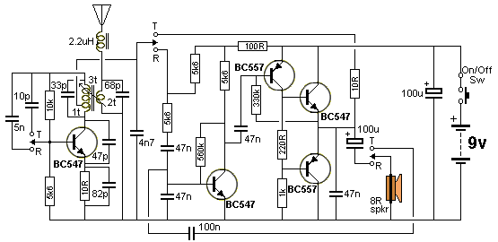
27MHz Walkie Talkie without Crystal
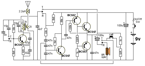
27MHz Walkie Talkie with Call
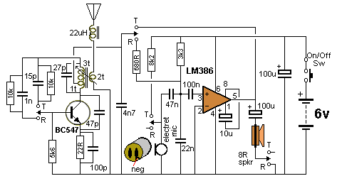
27MHz Walkie Talkie with LM386 Audio Amplifier
49MHz WALKIE TALKIES
Two bands have been allocated for walkie talkies and remote control equipment. These are the 27MHz band and 49MHz band. The 49MHz band has slightly better performance due to the short antenna being closer to the wavelength of the signal. The two bands allow more remote control cars to be raced together without interference between the cars.
FURTHER USES
All of these circuit can be found in remote-control toys from your local department store. Simply buy a remote control car and give it to a youngster to play with. After a day or two he will lose interest and you will be able to pull it apart and adapt it to your own use.
To create a private channel, simply replace the crystal with one of a slightly different frequency and retune both the transmitter and receiver coil. The multi-channel receiver has even most possibilities. You can control four different devices directly and even more by gating the outputs. The simple 27MHz link will be used with one of our Talking Electronics FM transmitters to turn it ON and OFF remotely.
The 27MHz transmitter will work up to 60ft (20m) and will allow you to turn off a transmitter to give it added security from being detected. The receiver will have to be designed to turn on for 0.5sec every 10 seconds to detect if a turn-on transmission is being sent and the whole circuit will then shut down to conserve power if a reception is not detected.
This means you will have to transmit for at least 10 seconds to be sure the receiver picks up the signal.
On the next page we cover some more 27MHz transmitter circuits, and on P3 we cover some 303MHz links.

Quick Links
Legal Stuff
Social Media