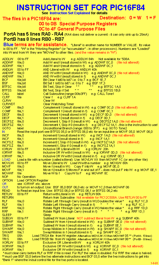
ADDITIONAL INSTRUCTIONS
ADDWF PCL,1 ADDWF 02,1 Alter the program counter to create a jump
CLRF INDF,1 CLRF 00,1 Clear INDIRECT file
INCF FSR,1 INCF 04,1 Increment the File Select Register
INTCON address is either 0Bh or 8Bh - it is mapped at both locations.
BCF INTCON,RBIF Clear RB<7:4> Port-change Interrupt flag
BSF INTCON,RBIF Set RB<7:4> Port-change Interrupt flag
BCF INTCON,RBIE Disables the Port-change Interrupt
BSF INTCON,RBIE Enables the Port-change Interrupt
BCF INTCON,INTE Disables the RB0/INT Interrupt
BSF INTCON,INTE Enables the RB0/INT Interrupt
BCF INTCON,T0IE Disables the TMR0 Interrupt
BSF INTCON,T0IE Enables the TMR0 Interrupt
BCF INTCON,EEIE Disables the EE write complete Interrupt
BSF INTCON,EEIE Enables the EE write complete Interrupt
BCF INTCON,GIE Disables all Interrupts
BSF INTCON,GIE Enables all un-masked Interrupts
OPTION address is 81h - use the word OPTION
OPTION,0 OPTION,1 OPTION,2
Prescaler Rate Select Bits
| Bit Value | TMR0 Rate | WDT Rate |
|---|---|---|
| 000 | 1:2 | 1:1 |
| 001 | 1:4 | 1:2 |
| 010 | 1:8 | 1:4 |
| 011 | 1:16 | 1:8 |
| 100 | 1:32 | 1:16 |
| 101 | 1:64 | 1:32 |
| 110 | 1:128 | 1:64 |
| 111 | 1:256 | 1:128 |
e:g:
BSF OPTION,0 BCF OPTION,1 BSF OPTION,2 TMR0 Rate = 1:64 WDT Rate = 1:32
BSF OPTION,0 BSF OPTION,1 BSF OPTION,2 TMR0 Rate = 1:256 WDT Rate = 1:128
BCF OPTION,PSA BCF OPTION,3 Prescaler assigned to TMR0
BSF OPTION,PSA BSF OPTION,3 Prescaler assigned to the WDT
BCF OPTION,T0SE BCF OPTION,4 Increment on low-to-high on RA4/T0CKI pin
BSF OPTION,T0SE BSF OPTION,4 Increment on high-to-low on RA4/T0CKI pin
BCF OPTION,T0CS BCF OPTION,5 Internal Instruction cycle clock (CLKOUT)
BSF OPTION,T0CS BSF OPTION,5 Clock source select. Transition on RA4/T0CKI Pin
BCF OPTION,INTEDG BCF OPTION,6 Interrupt on falling edge of RB0/INT Pin
BSF OPTION,INTEDG BSF OPTION,6 Interrupt on rising edge of RB0/INT Pin
BCF OPTION,RBPU BCF OPTION,7 PORT B Pull-ups are enabled
BSF OPTION,RBPU BSF OPTION,7 PORT B Pull-ups are disabled
STATUS address is either 03h or 83h - it is mapped at both locations.
BTFSS STATUS,C or BTFSC 03,0 Test the carry bit. C=1=set = carry occurred
BTFSS STATUS,C or BTFSC 03,0 Test the carry bit. C=0=reset = carry did not occur
BTFSS STATUS,DC BTFSS 03,1 Test the digit carry bit. C=1=set = carry-out from the 4th lower order bit of the result occurred.
BTFSS STATUS,DC BTFSS 03,1 Test the digit carry bit. C=0=reset = carry-out did not occur from the 4th lower order bit of the result.
BTFSS STATUS,Z or BTFSC 03,2 Test the zero bit. Z=1=set = result of arithmetic or logic operation is zero.
BTFSS STATUS,Z or BTFSC 03,2 Test the zero bit. Z=0=reset = result of arithmetic or logic operation is not zero.
BSF STATUS,RP0 BSF 03,5 Go to Bank1 for TRISA or TRISB register
BCF STATUS,RP0 BCF 03,5 Go to Bank0 for programming
CLRF INDF,1 CLRF 00,1 Clear INDIRECT file
RETFIE Return from Interrupt Sets INTCON,GIE
| File name: | File No: | Comments: |
|---|---|---|
| EECON1 | equ 088h | ;EEPROM Control Register 1 |
| EECON2 | equ 089h | ;EEPROM Control Register 2 |
| EEADR | equ 9 | ;EEPROM address Register |
| EEDATA | equ 8 | ;EEPROM Data Register |
| FSR | equ 4 | ;File Select Register |
| INDF | equ 0 | ;INDIRECT file |
| INTCON | equ 0Bh | ;Interrupt and Timer bits |
| OPTION | equ 081h | ;Option Register |
| PCL | equ 2 | ;Program Counter Low-bits |
| PORTA | equ 5 | ;Port A |
| PORTB | equ 6 | ;Port B |
| STATUS | equ 3 | ;Status Register |
| TRISA | equ 085h | ;Make Port A bits input or output |
| TRISB | equ 086h | ;Make Port B bits input or output |
| Bit name: | Bit No: | Comments and name of file holding the bit: |
|---|---|---|
| Carry | equ 0 | ;Carry bit in Status file C=0=no carry-out |
| DC | equ 1 | ;Digit Carry in Status DC=0=no carry out from 4th low-order digit |
| EEIF | equ 4 | ;In EECON1 EEIF=1=The write operation completed |
| f | equ 1 | ;Place the result of the operation in the file |
| GIE | equ 7 | ;Global Interrupt Enable bit. In INTCON 0=Disables all interrupts |
| RD | equ 0 | ;In EECON1 Read Control bit |
| RP0 | equ 5 | ;In Status. Register Bank select RP0=clear=bank0 RP0=set=bank1 |
| Self | equ 1 | ;Store the result in the file |
| T0IE | equ 5 | ;In INTCON Timer0 Overflow Interrupt Enable bit |
| T0IF | equ 2 | ;In INTCON Timer0 Overflow Interrupt Flag bit |
| W | equ 0 | ;Place the result in W |
| WR | equ 1 | ;In EECON1 Write Control bit |
| WREN | equ 2 | ;In EECON1 EEPROM Write Enable bit |
| Z | equ 2 | ;Z in Status file. Zero flag=set=1 when result of operation is zero!! |
Quick Links
Legal Stuff
Social Media


