

Table Of Contents
Essential for servicing all types of Digital circuits
This LOGIC PULSER capable of delivering pulses of various compositions, to any type of circuit you wish to test.
Basically it is designed to complement the LOGIC PROBE and can be used in situations where the LOGIC PROBE is not so effective.
It is an improvement over a multimeter in that it has an audible output and is NOT triggered when measuring across a diode. Don’t underestimate the importance of this item of test equipment. It is needed to properly test and locate a fault in digital circuits.
The time when you appreciate it most is when a tricky fault comes along.
We have had a number of these and know how difficult it is to improvise.
A multimeter and CRO are all right for some applications but when it comes to testing digital circuits, they can give a readout which can be incorrectly interpreted and cause you to branch in the wrong direction.
The right tool for the right job is the answer and this is specifically designed for digital circuits.
The value of a LOGIC PULSER is not immediately obvious. You may think a probe is sufficient for all situations.
This is not so. Some circuits require to be tested in sections. This means the input waveform is not present and you require to know if the circuit will process the signals when it all goes together. This is the case for a logic pulser.
It is capable of delivering pulses to a circuit so that the result(s) can be detected, even though the circuit may not be complete.
The pulser has a wide range of output frequencies, ranging from 1Hz to 800Hz. Between these there are a number of output values which have varying mark-space ratios. The waveform, in all cases, has a fast rise and fall characteristic, making it ideal for injecting into chips.
The output transistor in the probe is protected via a 1k resistor so that you can place the tip on any pin of an IC and not damage either chip or probe.
HOW TO USE THE LOGIC PULSER
Connect the positive and negative leads of the pulser to the power rails of the project under test.
Turn the project ON and this will also supply power to the pulser.
Depending on the fault you are tracing, the frequency of the pulser (and the result you will get), will vary. In fact there are so many different effects that we could not list them all. This is because the probe has a varying mark-space ratio which will create different effects in different circuits.
USING THE PULSER
The logic pulser can be used by itself if the project you are testing has output devices which show the results of the signals.
If output indicators are not available, you will have to use the logic probe described in issue 10.
The basic method of using the logic pulser is as follows:
Place the pulser on each of the pins of the chip and detect the effect on the output via the logic probe.
You may or may not get a reading. This will depend on how firmly the input lines are ‘tied’ to the rails.
This may sound unusual but it is an unfortunate fact for digital circuits. If you take the simple case of a chip being clocked by the output of another, the clock line is being taken HIGH and then LOW during the operation of the circuit.
If you halt the circuit when the output is LOW, it will be very difficult to pull the line HIGH because it is being kept LOW by the output transistors of the driving chip.
These transistors have a certain amount of ability to keep the line LOW and this is called SINKING ABILITY. For TTL this can be as much as 45mA and for CMOS it will be up to about 25mA.
This means we would have to put a signal on the line and deliver more than 25 mA or 45mA to pull it HIGH.
The output transistors would not like this and having a capability of delivering 45mA to a circuit could prove to be damaging to lots of other parts of the circuit.
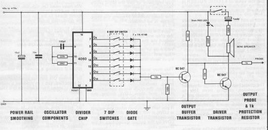
The LOGIC PULSER is built around a CD 4060, 14-stage divider chip which has an inbuilt oscillator. With the addition of 3 components, the oscillator drives a string of 14 flip flops. The first output pin comes from the output of the 4th flip flop and this means the clock frequency is divided by 8.
From there it is divided further and an output is available from flips flops 5 to 14 (except 12).
We have used Q4, Q5, Q6, Q8, Q10, Q12, and Q14 in our project and have found these to be the most suitable for producing pulse trains.
Each output of the chip is taken to a switch on the 8-way DIP switch package and then diode gated together to form an OR gate.
A transistor buffer passes the signal to the probe tip where a 1k resistor is present to prevent damage to the probe if probing a power rail etc.
By turning ON various combinations of switches, you can produce a wide range of tones from a whistle to a 1Hz pulse.
You can modulate the tone by tuning on additional switches to produce ‘chirping’ or ‘phone-ringing’ tones. This has the effect of delivering a HIGH pulse modulated by LOW pulses, at the same time.
CONSTRUCTION
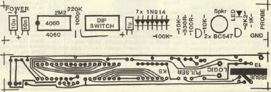
The PULSER is constructed on a single-sided PC board and assembled in the normal way.
Because the PC must be inserted into a toothbrush case, the components must be small and any tall components must be bent over to lay flat against the board.
There is nothing ‘special’ or ‘unusual’ about assembly and construction is straight-forward providing you have a fine tipped soldering iron.
The IC lands are circular due to the compact nature of the layout and you must be careful when inserting the IC socket.
All components must be pushed hard against the PC board before soldering so that they take the least height possible. The two electrolytics, however, and 10n greencap must be kept slightly above the board so that they can be bent over and lay flat.
Start assembly by inserting the IC socket. If the socket has a cut-out indicating pin 1, place this over the ‘dot’ on the overlay.
Next fit the two links. They are positioned near the end of the 1C socket. The second link is NOT straight but shaped like the letter ‘L’. This has been necessary due to the compact nature of the layout.
Next fit the 7 gating diodes. These all face the same way and are pressed firmly against the board before soldering.
Between the diodes and the end of the board are 7 resistors (and a mini speaker). The resistors fit flat against the board and are soldered in place.
The two BC 546 or 547 or 548 transistors are pushed nearly up to the board and soldered in place.
The 3mm LED is the next to be placed on the board and it must be inserted the correct way for it to operate.
Insert the mini speaker and solder it in place. It can be fitted around either way.
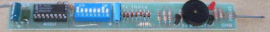
Only a few components remain. Start with the DIP switch. It is soldered directly to the board so that the numbers on the switches can be read as per the photo.
Solder the two electrolytics so that the leads can be bent over and allow them to lay flat against the board. The 10u electrolytic fits near the end of the board and the 1mfd near the middle.
The 10n greencap also lays flat against the board. Make sure there is sufficient lead for this to be done.
Finally the two resistors and 100pf ceramic are fined to the board. The resistors stand ON END to occupy the least space.
The power leads which supply the pulser with energy should be about 50cm long to give you plenty of freedom when using the unit. Solder alligator clips or E-Z clips to the ends. Before connecting the leads to the board, push them through two holes in the end of the case and then solder to the board.
Straighten out a paper clip and solder it to the end of the board to form a probe. Insert the 4060 IC and the project is ready for testing.
TESTING
Connect the probe to a power source. This can be a voltage from 5v to 15v. Determine which way the switches must be clicked for them to be ON so that you know how many switches are needed to achieve a particular pulse train.
Switch number 1 turns on the speaker, all others modulate the output.
Turn on switch “1” and any of the others. You will hear a tone in the speaker. If no tone is heard, try different combinations and observe the LED. If it blinks on and off, the fault will lie in the speaker circuit: made up of the speaker, 100R resistor, 1u electrolytic and switch 1. If the LED remains ON, the fault will lie in the chip and oscillator stage. If the LED remains OFF the fault may lie in the driver transistor.
To determine the operation of the 4060, connect our LOGIC PROBE, to the power rails and probe output pins 1, 2, 4, 5, 7, 14 and 15.
If no pulses are detected on these pins, the 4060 may not be oscillating. This could be due to the 3 frequency setting components not being wired into the circuit correctly, pin 12 not being connected to 0v or pin 16 not being connected to positive rail. Also look for shorts between pins 9, 10 and 11.
If a signal is present on the cathode end of the diode but not on the probe tip, the fault will lie in the buffer (amplifier) transistor. You cannot probe the base of the transistor with the Logic Probe as the voltage swing is not sufficient to be detected.
The transistor may be at fault or you may have a short between base and emitter. It could also be the 2k2 resistor may not be connected to the collector.
When there is no tone being produced by the pulser, the light emitting diode is illuminated, indicating the probe tip is HIGH.
The pulser can then be used as a HIGH to test various components, remembering it has a safety resistor in series with the tip to limit the current.
ASSEMBLY
The PULSER is designed to fit into a toothbrush case. You will have to look around your local chemist for an injection-moulded polystyrene case with the correct dimensions. Don’t get a blow-moulded case or fabricated case as they don’t have the rigidity.
The spring-steel probe tip is passed through a small hole in the end of the case and the two power leads through two holes at the other end.
Close the case and you will find the switches cannot be adjusted.
With a hot soldering iron, mark a rectangle above the switches, large enough to get the tip of your finger through. If you prefer, you can make the cut-out smaller and use a screwdriver to flick the switches.
Remove the board and fit the two halves of the case together. Use the tip of the soldering iron to cut through the plastic and create the cut-out. You can finish the edges with a file but make sure you don’t fracture the case.
Insert the PC board and close the case again. Use clear sticky tape around the join and cut around the rectangular opening with a blade.
The probe is now ready to go to work on the next faulty project.
Let’s hope that’s soon!
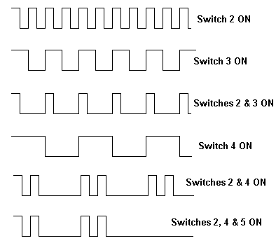
These CRO diagrams show the effect of turning ON various switches. The correct combination
is obtained by experimentation and you will get different effects on the output of the chip you are testing, as the switches are altered. The most noticeable differences will occur when a capacitor is present in the circuit under test as it will will introduce a delay factor.
LOGIC PULSER - PARTS LIST
1 - 100R
1 - 330R1 - 1k
1 - 2k2
2 - 10k
1 - 100k
1 - 220k
1 - 2M2
1 - 100pf
1 - 10n greencap
1 - 1u electro
1 - 10u electro
7 - 1N 4148 diodes
1 - 3mm red LED
2 - BC 547 transistors
1 - CD 4060 IC
1 - mini speaker
1 - 8-way DIP switch
1 - 16 pin IC socket
1 - 5cm tinned copper wire
1 - paper clip for probe tip
1 - 50cm red hook-up flex
1 - 50cm black hook-up flex
1 - red EZY-CLIP
1 - black EZY-CLIP
1 - PULSER PC BOARD

Quick Links
Legal Stuff
Social Media