Table Of Contents
TRUTH TABLE

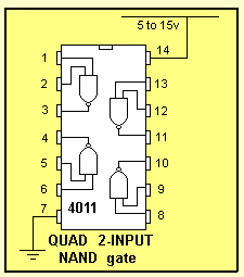
- The CD 4011 is the most used CMOS chip.
- It contains 4 NAND gates.
- Minimum supply voltage 3v
- Maximum supply voltage 15v
- Max current per output 10mA
- Maximum speed of operation 4MHz
- Current consumption approx 1uA

Follow the inputs and note when the LED is illuminated.
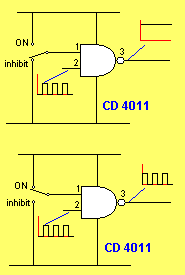
GATING
The secret to understanding the operation of
the gate is show in the diagram on the right.
It is called GATING.
When one input is held LOW, the output is a constant HIGH.
When one input is held HIGH, the signal on the other input will be inverted by the gate and appear on the output.
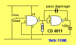
This is also shown in the 1kHz tone circuit below.
Note:
Do not leave an input “open” (non-connected) as the high input impedance (approx 10M) will pick up noise and create faulty operation.
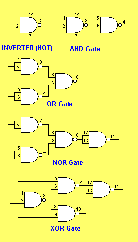
The CD 4011 IC has 4 gates and these can be wired to create a BUFFER, Inverter (NOT), AND, OR, NOR XOR or XNOR. In most cases this will use 3 or 4 of the gates and represents a wasteful use of the chip. These examples are useful for demonstration purposes:
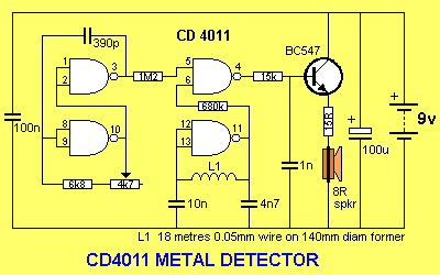
Circuits built around a CD 4011:
Quick Links
Legal Stuff
Social Media


