Table Of Contents
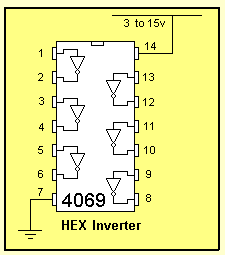
- The 4069 contains 6 Inverters.
- Minimum supply voltage 3v
- Maximum supply voltage 15v
- Max current per output 10mA
- Maximum speed of operation 4MHz
- Current consumption approx 1uA with nothing connected to the inputs or outputs.
Connect any unused inputs to 0v rail.
Current consumption with inputs left “floating” (non-connected) = 600microamps.
Current consumption with all inputs connected to 0v = 1microamp.
See: Wireless Doorbell for a project using this chip.

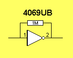
To turn an inverter into an amplifier, a 1M resistor is connected between input and output.
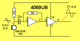
Each inverter has a gain of approx 20 in the diagram above.
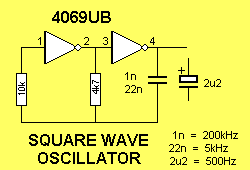
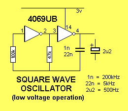
A square wave oscillator can be made from 2 inverters.
You need to use high impedance components for the chip to work on low voltage.
The following circuit shows this:
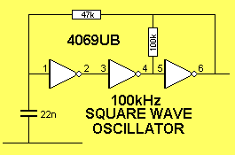
A square wave oscillator can be made from 3 inverters.
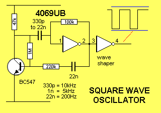
A square wave oscillator can be made from a single inverter and a transistor. The second inverter shapes the wave to produce a square wave.
SOME BACKGROUND THEORY
The pinout of a 4069UB and 74C14 are identical.
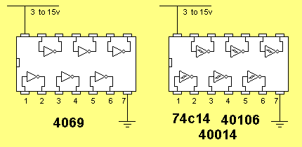
Both chips have the same driving capability - about 5 - 10mA per output for a voltage 6v or higher.
If you need a larger driving current, use a transistor “buffer” called a Driver Transistor.
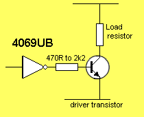
The main difference between the two chips: Each inverter in a 4069 will amplify a very small analogue signal (less than 1mV) and produce an analogue output. It will have a gain of approx 20.
The 74c14 has six Schmitt trigger Inverters. Each inverter will change state when the input rises from a low level to above 66% of rail voltage and change to the opposite state when the input voltage falls from a high level to below 33% of rail voltage.
The gap between 34% and 65% is called the Hysteresis Gap and cannot be altered. Any signal that moves between 33% and 66% of rail voltage, will not cause the output to change. A signal that rises above 66% and falls below 33%, will cause the output to change.
The output has only two states. 0v or rail voltage. The chip has a DIGITAL OUTPUT.
See Page 49 and Page 76 of Basic Electronics Course for details on how to use the 74c14.
THE 4069
The 4069 has an ANALOGUE OUTPUT when configured as an amplifier (as shown above).
If one of the inverters of a 4049 has no components connected between output and input, the output will go LOW when the input reaches mid-rail voltage. When the input voltage falls slightly below mid-rail, the output will go HIGH. This change occurs when the input voltage changes by only a few millivolts.
GATING AN OSCILLATOR
An oscillator can be made to turn ON and OFF via a “gating signal.” This gating signal can be a push button or a pulse from the output of another gate.
In the diagram below, the high-frequency oscillator (the second section), is gated via the low-frequency oscillator:
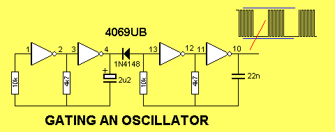
When the gating diode is placed as shown in the diagram above, the output is LOW when the oscillator is gated (frozen). If the gating diode is reversed, the output will be HIGH when the oscillator is frozen.
Quick Links
Legal Stuff
Social Media


